ASIA ELECTRONICS INDUSTRYYOUR WINDOW TO SMART MANUFACTURING
IC Process Materials Makers Invest Actively in EUV
Japanese semiconductor process materials manufacturers have been stepping up investments eyeing full-fledged adoption of extreme ultraviolet (EUV) technology, the next-generation lithography technology. They aim to contribute to the development of the semiconductor industry by bankrolling investments to bolster production capacities for EUV-related materials and through other strategic investments.
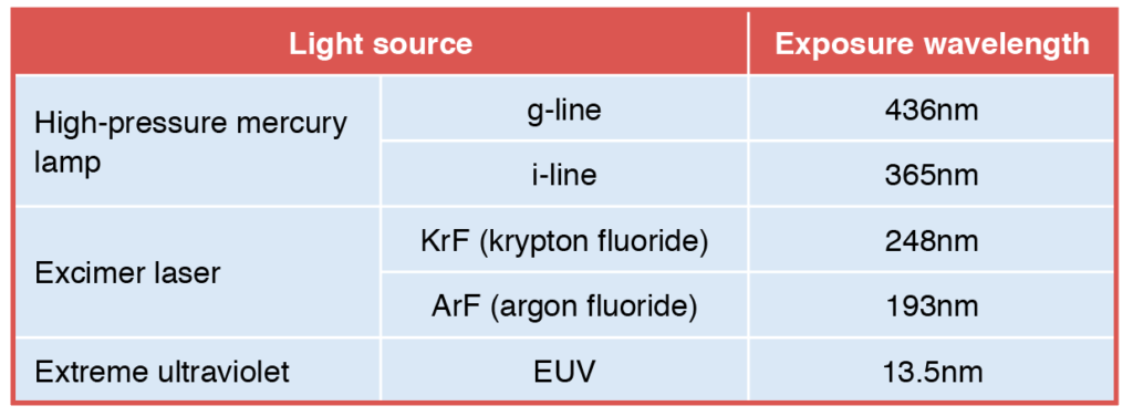
With the full-fledged emergence of internet of things (IoT), artificial intelligence (AI), and and the start of the commercial services of fifth-generation communications standard, semiconductor chips are required to provide faster computing, larger data capacities and higher integration. In order to meet these requirements, it is necessary to achieve finer semiconductor circuit patterns. However, the conventional photolithography technology using excimer laser has its own limitations, and EUV lithography technology attracts attention as a cutting-edge microfabrication technology replacing excimer laser lithography.
EUV lithography uses EUV light with a wavelength of 13.5nm as a light source, enabling the formation of several-nanometer circuit patterns on silicon wafers. Some semiconductor manufacturers have begun to use EUV lithography in leading-edge 5 to 7nm processes, and the market expected is to grow dramatically.
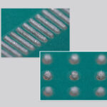
Given this backdrop, semiconductor process materials manufacturers have been accelerating the technological development of next-generation photoresists (sensitive materials), pellicles (dustproof covers for photomasks), and mask blanks, setting their sights on EUV lithography. In addition, they have also embarked on investments in plants and equipment for these products, anticipating surge in demand.
Bolster Capability
Tokyo Ohka Kogyo Co., Ltd. has been actively investing to expand its semiconductor photoresist business. As a medium-term goal, the company targets to increase the sales of advanced resists (EUV+ArF) in FY2021 (ending December) to almost 140 percent of its sales in FY2018. The company expects sales of EUV photoresists in FY2020 to almost double those in FY2019. To supply high-quality materials, the company is building a new clean room at the Sagami Operation Center in Kanagawa Prefecture, Japan, with operation slated to begin this year.
Sumitomo Chemical Co., Ltd. announced in spring that it will build a new building at Osaka Works in Osaka and install new evaluation equipment in order to strengthen its development and quality assurance system for semiconductor photoresists for EUV lithography and other advanced semiconductor processes. This project is due to be completed in the first half of FY2022.
By constructing a new building equipped with clean rooms and introducing new exposure equipment, the company will increase its development efficiency of EUV photoresists and accelerate its response to customers, while further enhancing the quality assurance system. The company will also consider further investment in line with the future expansion of business in the cutting-edge photoresists area including EUV.
In 2019, Mitsui Chemicals, Inc. concluded a licensing agreement on the EUV pellicle business with ASML, the No. 1 company worldwide in the field of semiconductor lithography systems, acquiring production rights and production and sales rights for EUV pellicles. Based on this agreement, Mitsui Chemicals started building an EUV pellicle assembly factory at Iwakuni Otake Works in Yamaguchi Prefecture with target completion by Q2 (July to September) of FY2020. The company aims to start operating the factory for commercial offering by Q2 of FY2021.
Expand Production
AGC Inc. has decided to aggressively expand a supply system for EUV lithography photomask blanks (EUVL mask blanks) at its group company, AGC Electronics Co., Ltd. in Fukushima Prefecture, Japan. The construction including building expansion is supposed to start in October and operations are scheduled to start in 2022.
In 2017, AGC started producing EUVL mask blanks. The company has made necessary investments to meet market demand. To respond to further expansion of the EUV lithography market, this time, it has decided on the drastic expansion of the supply system for EUVL mask blanks. As the only manufacturer of EUVL mask blanks that can handle every aspect from glass materials to coating, AGC will establish a mass production system to meet growing market demand, with the aim of achieving target sales of ¥40 billion or more and a global market share of 50 percent in 2025.
Equity Investment
JSR Corporation announced in February that it has made additional contribution to Inpria Corporation in Oregon, the United States. JSR took part in Series C Funding newly solicited by Inpria with the aim of commercializing the company’s EUV photoresists. Since its inception, Inpria has been working on the development of EUV photoresists that include non-chemical amplified metals. Its photoresists, which include tin-oxide as the main component, have achieved limit resolution that is the highest performance for photoresists for EUV lithography. Through its funding contribution, JSR will collaborate with Inpria in diverse aspects of EUV photoresists development, and accelerate efforts toward the commercial offering of EUV photoresists.
Note:
EUV: Extreme ultraviolet radiation with a wavelength of 13.5nm (1n=one billionth).
- Share: