ASIA ELECTRONICS INDUSTRYYOUR WINDOW TO SMART MANUFACTURING
Lasertec Highlights EUV Inspection Systems
At SEMICON Taiwan 2023, Lasertec Corporation highlighted inspection systems for extreme ultraviolet (EUV) lithography, focusing on EUV lithography. The company also proposed measurement equipment that supports the ongoing development of advanced packaging technologies. By offering these systems, Lasertec aims to boost the technological evolution of state-of-the-art semiconductors.
At its booth, Lasertec showcased the ACTIS A150 Actinic EUV patterned mask inspection system, the first to adopt EUV light on a panel. The company introduced the MATRICS X9ULTRA mask inspection system and other systems on panels.
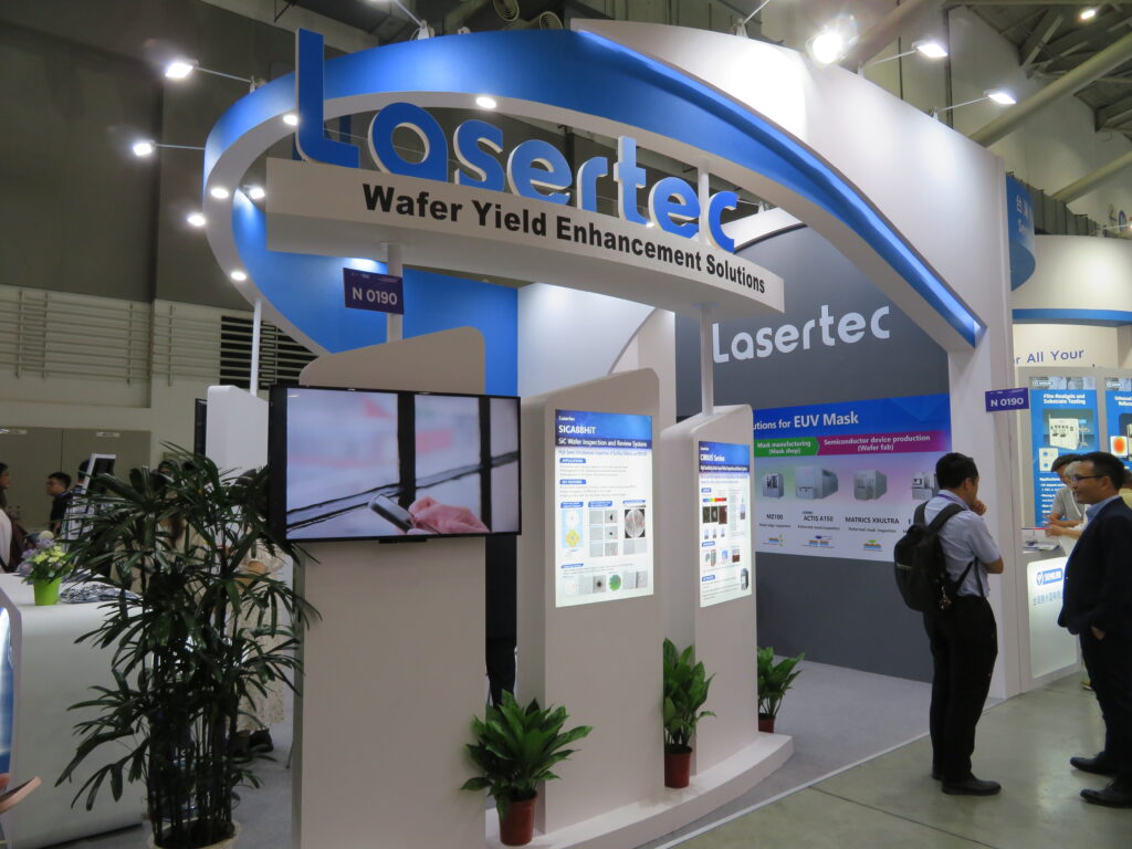
Mainly, A150 demonstrates far greater performance than conventional mask inspection systems that use deep ultra-violet (DUV) laser. Thus, it provides higher detection sensitivity and enables the detection of printable phase defects unique to EUV masks. Also, it has the ability to inspect EUV masks with pellicles attached. The installation of A150 has been progressing mainly at mask shops.
Koichi Moriizumi, Director, Senior Managing Executive Officer, Lasertec, said, “With the advancement of process node toward 2nm, the EUV market will expand. We will propose MATRICS X9ULTRA targeting fabs that use EUVs without pellicles. This way, Lasertec implements multi-directional strategies.”
Advanced packaging technologies, such as chiplets, have been progressing. In keeping with the advancement of packaging technologies, wafer processing technologies are also becoming more complex and sophisticated. Chip on wafer on substrate (CoWoS) 2.5D packaging technology using through silicon vias (TSV) are adopted. Meanwhile, TSVs will expand in the coming years.
Also, at SEMICON Taiwan, the BGM300X TSV back grinding process measurement system attracted much attention.

Tetsuya Sendoda, Executive Officer, Lasertec, said, “The combination of Lasertec’s proprietary interferometer and infrared (IR) optical system enables high-precision measurement of via etching depth. This technology is optimum for the back grinding process and the thickness measurement of silicon (Si) after etching.”
Sendoda continued, “Advanced packages require complex technologies, such as the reduction of wafer thickness and heterogeneous integration, and therefore, the measurements of thicknesses and unevenness are important. Lasertec will pay attention to development trends of leading-edge technologies, such as the miniaturization and three-dimensional (3D) high integration, to contribute to the development of state-of-the-art semiconductor technologies.”
- Share: