ASIA ELECTRONICS INDUSTRYYOUR WINDOW TO SMART MANUFACTURING
SK Hynix to Brace for Mass Production of HBM4
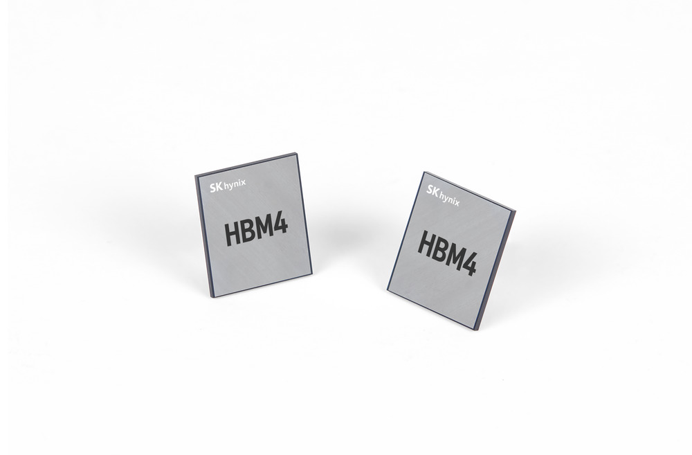
SK hynix has completed the development of the industry’s first HBM4 of next-generation memory product. Accordingly, the new HBM4 targets ultra-high performance AI applications.
Following the development completion, SK hynix is preparing HBM4 into mass production to lead address the challenges of AI era. Through this momentum, the company has once again proven the AI memory leadership in the global market.
“Completion of HBM4 development will be a new milestone for the industry,” said Joohwan Cho, Head of HBM Development at SK hynix. “By supplying the product that meets customer needs in performance, power efficiency and reliability in timely manner, the company will fulfill time to market and maintain competitive position,” said Joohwan, who led the development team.
Meets Demands of AI Applications
The need for high bandwidth memory for faster system speed has become even more necessary with the dramatic increase of AI demand and data processing. Moreover, memory power efficiency is also emerging as a key requirement for customers with the increasing power consumption of data center operation.
Therefore, SK Hynix has developed HBM4 to address the need for drastic increase in bandwidth and power efficiency.
SK hynix’s HBM4 is a high-value, high-performance memory that vertically interconnects multiple DRAM chips and dramatically increases data processing speed compared to conventional DRAM products.
HBM4 has the industry’s best data processing speed and power efficiency with the bandwidth doubled through adoption of 2,048 I/O terminals, double from the previous generation. Furthermore, power efficiency also improved by more than 40%. The company expects HBM4, when employed, can improve AI service performance by up to 69%. Thus, leading to solve data bottleneck and significantly reduce data center power costs.
SK hynix has far exceeded the JEDEC3 standard operating speed of 8Gbps by implementing over 10Gbps operating speed in HBM4.
MR-MUF: Critical to Mass Production
In addition, the company adopted the Advanced MR-MUF process in HBM4, which has been proven to be reliable in the market. MR-MUF, or Mass Reflow Molded Underfill, protects the circuit between chips and hardening them. It is the process of stackings semiconductor chips, injecting liquid protective materials between them.
The process has proved to be more efficient and effective for heat dissipation, compared with the method of laying film-type materials for each chip stack. SK hynix’s advanced MR-MUF technology is critical to securing a stable HBM mass production as it provides good warpage control and reduces the pressure on the chips being stacked.
In addition, it also integrates the 1bnm process, or the fifth-generation of the 10-nanometer technology, to minimize the risk in mass production.
Justin Kim, President & Head of AI Infra at SK hynix, said, “HBM4, a symbolic turning point beyond the AI infrastructure limitations, will be a core product for overcoming technological challenges. We will grow into a full-stack AI memory provider by supplying memory products with the best quality and diverse performance required for the AI era in a timely manner.”
15 September 2025
- Share: