ASIA ELECTRONICS INDUSTRYYOUR WINDOW TO SMART MANUFACTURING
Siemens' New Design Kit Boosts Samsung Foundry Design
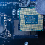
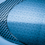
Siemens Digital Industries Software has announced the availability of a new process design kit (PDK) from Samsung Foundry. Particularly, it helps mutual customers boost the reliability, quality, and robustness of their next-generation IC designs manufactured using the foundry’s latest processes.
Particularly, the design kit supports Siemens’ Calibre® DesignEnhancer software solution. This is the latest addition to the company’s EDA industry-leading Calibre® nmPlatform for IC verification.
Unveiled in July at the 2023 Design Automation Conference, the Calibre DesignEnhancer solution provides multiple-use models that perform automatic layout optimizations. Moreover, they improve power robustness and reduce design cycles during design implementation.

Faster Turnaround Time
Furthermore, the Calibre DesignEnhancer works with the Samsung PDK to help mutual customers achieve substantial first-pass gains in designer productivity when compared to traditional place-and-route (P&R) processes. Often, they require design teams to conduct multiple runs to achieve the same Calibre nmDRC-correct results.
“Samsung Foundry has a long and successful track record of leveraging Siemens’ Calibre software to provide our mutual customers with ‘Calibre nmDRC-correct’ designs. Based on the results we have seen, the Calibre DesignEnhancer solution provides our mutual customers with a step function increase via insertion efficiency. (Also), faster turnaround time compared to classic approaches to the problem,” said JoongWon Jeon, Distinguished Engineer of the Foundry Technology Development Team at Samsung Electronics.
The Calibre DesignEnhancer via insertion use model automatically inserts additional Calibre nmDRC-correct vias into layouts to reduce the resistance that can minimize both voltage (IR) drop and electrostatic discharge (ESD) events in IC designs. Furthermore, the Calibre DesignEnhancer via optimization use model can add up to millions more vias than previously possible.
“The incorporation of the Calibre DesignEnhancer solution with Samsung Foundry’s most advanced processes demonstrates what can be possible when world-class IC EDA and fabrication players partner to help mutual customers successfully and efficiently fabricate new devices in leading-edge technologies,” said Michael White, senior director, Physical Verification Product Management, Siemens Digital Industries Software.
- Share: