ASIA ELECTRONICS INDUSTRYYOUR WINDOW TO SMART MANUFACTURING
Lasertec Releases New EUV Patterned Mask Inspection System
Lasertec Corporation has released the ACTIS A300 Series actinic EUV patterned mask inspection system for high-numerical aperture (NA).
Over time, the semiconductor industry keeps improving its manufacturing processes. Specifically, it pusues production of smaller-geometry devices to achieve higher performance, faster speed, and better energy efficiency.
Lasertec’s ACTIS A150 actinic EUV patterned mask inspection system has been facilitating the adoption of EUV lithography to high-volume manufacturing. It is renowned for its excellent inspection performance in the industry today.
The newly released ACTIS A300 is a next-generation model that meets the requirements of manufacturing processes using high-NA EUV lithography. Specifically, it enables the further miniaturization of device geometries. Additionally, the A300 Series uses newly designed optics and high-brightness light source URASHIMA. Accordingly, it achieves a significant improvement in defect detection performance compared to the A150 Series.
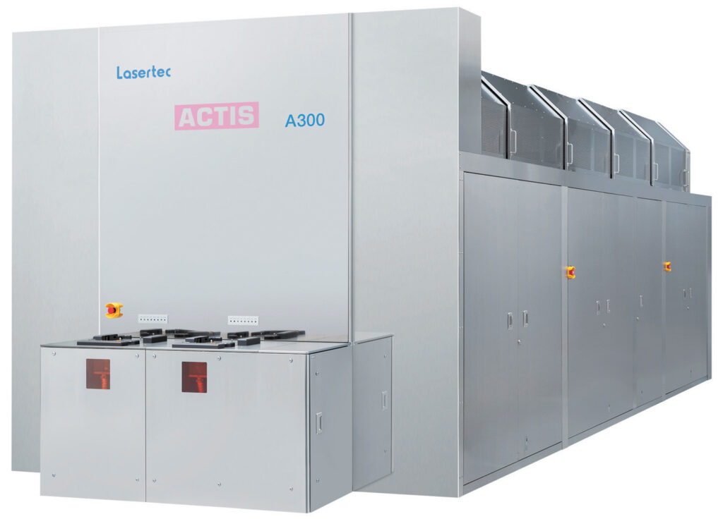
The anamorphic optics used in high-NA lithography adopted different magnifications of projection in the X and Y directions. Therefore, inspection of EUV masks for high-NA lithography, requires different levels of resolution in the two directions. The A300 Series is also applicable for inspection of EUV masks for the current NA lithography as well as EUV masks for high-NA lithography.
Lasertec supports the needs of leading-edge semiconductor manufacturers. In relation, it will develop unique solutions and facilitate quality and productivity improvement, thereby contributing to the advancement of the industry.
Key Features of ACTIS 300
The ACTIS 300 Series enables inspection of EUV masks for high-NA lithography and EUV masks for the current NA lithography. Also, it offers high productivity inspection with highly efficient optics and high-brightness light source URASHIMA.
The latest mask inspection system is used for quality assurance inspection during EUV mask manufacturing processes. Also, it suits incoming EUV mask inspection and periodic quality assurance inspection at wafer fabs.
