ASIA ELECTRONICS INDUSTRYYOUR WINDOW TO SMART MANUFACTURING
Keysight Introduces New Chiplet PHY Designer
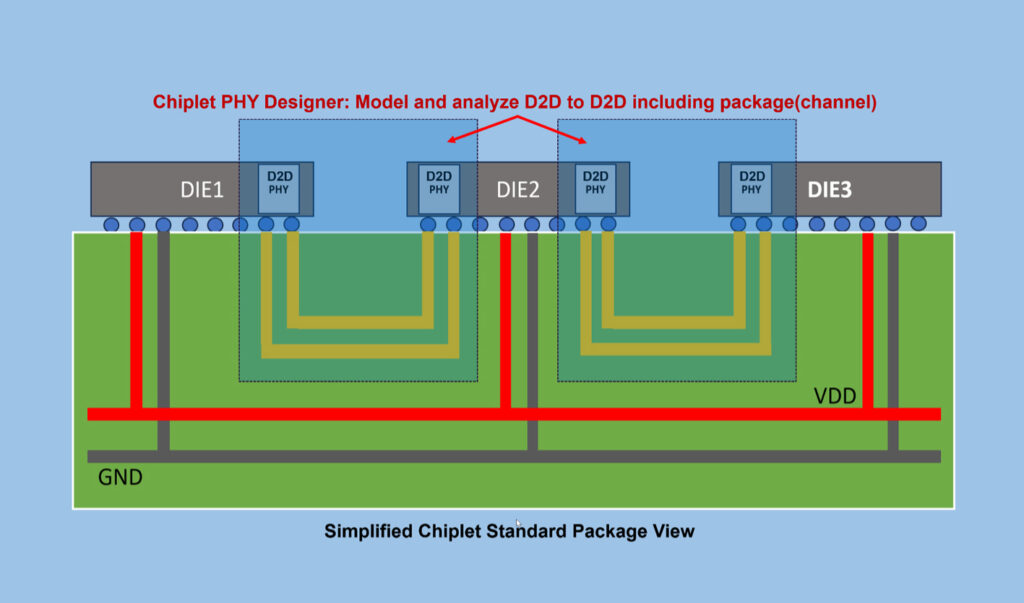
Keysight Technologies, Inc. introduces Chiplet PHY Designer, the latest member in its family of high-speed digital design and simulation tools. Accordingly, it provides die-to-die (D2D) interconnect simulation, which is a key step in verifying performance for heterogeneous and 3D IC designs commonly referred to as chiplets.
The new electronic design automation (EDA) tool is the industry’s first to provide in-depth modeling and simulation capabilities. Specifically, it enables chiplet designers to rapidly and accurately verify that their designs meet specifications of the Universal Chiplet Interconnect Express™ (UCIe™) standard.
UCIe is emerging as the leading chiplet interconnect specification in the semiconductor industry. It is an open standard that defines the interconnect between chiplets within an advanced 2.5D or 3D package. Moreover, UCIe is in the process of gaining support or adoption by many of the top semiconductor equipment and EDA tool vendors. Particularly, foundries and chiplet designers.
Designers who use the interconnect standard and ensure their chiplets perform to its specifications. In addition, help establish a broad ecosystem for chiplet interoperability and commerce.
Aligned With Industry Standard
Keysight EDA’s research and development team has been working on modeling and simulating high-speed digital interfaces. For example, ADS Memory Designer offers comprehensive memory interface coverage such as GDDR7, DDR5, LPDDR5, and HBM3 with its IBIS-AMI modeler. Its rigorous and genuine JEDEC compliance test solution handles over 100 test IDs with the same test algorithm found in the Keysight Infinium oscilloscope family.
Key features of the Chiplet PHY Designer physical-layer simulator include:
- Supports UCIe physical layer standard
- automated parsing of signals following the standard naming conventions
- automated connections between multiple dies through package interconnects
- standard driven simulation setup such as speed grade
- intuitive measurement setup through specialized probe component
- Measurement of voltage transfer function (VTF)
- precisely computes a VTF to ensure UCIe specification compliance and analyzes system bit error rate (BER) down to 1e-27 or 1e-32 levels
- measures eye diagram height, eye width, skew, mask margin, and BER contour
- Analysis of forwarded clocking to accurately capture the asynchronous clocking behavior
Critical to System Design, Performance
Adrien Auge, Senior Staff Applications Engineer, Alphawave Semi, said validating Alphawave Semi’s chiplet solutions is crucial for enabling a future of heterogenous chip design. Particularly, Auge said it ensures seamless operation and interoperability for 2.5D/3D solutions available to our customers.
In addition, Auge said, “Chiplet PHY Designer simplifies the electrical simulation process for large die-die electrical connectivity, such as UCIe. It provides engineers and designers a quick and easy path to extract electrical compliance of their solutions against the latest revision of the specification. Furthermore, by complying with the latest IBIS modeling specification for electrical I/O, physical integrators can delve deeper into the chiplet electrical validation process, leveraging our detailed models to obtain pre-silicon performance predictions.”
Meanwhile, Niels Faché, Vice President and General Manager, Keysight EDA, said, “Our high-speed digital simulation team capitalized on its understanding of the shift left challenges presented by SerDes PHYS. They have applied these learnings to the chiplet domain to extend success of our standards-based simulation strategy to UCIe.”
Faché said interconnect modeling is critical to system design and performance. Thus, Chiplet PHY Designer accelerates validation of chiplet subsystems, from one D2D PHY through interconnect channels to another D2D PHY. Moreover, it enables 3D IC designers to solve critical interconnect performance problems improving predictive virtual prototyping to speed time-to-market.
- Share: