ASIA ELECTRONICS INDUSTRYYOUR WINDOW TO SMART MANUFACTURING
New Investments to Bring Advanced Nano-equipment to MIT.nano
MIT and Applied Materials, Inc. agreed to commit more than US$40 million of estimated private and public investment to add advanced nano-fabrication equipment and capabilities to MIT.nano. The investment includes a grant to MIT from the Northeast Microelectronics Coalition (NEMC) Hub. MIT.nano is the Institute’s center for nanoscale science and engineering.

Specifically, the collaboration will create a unique open-access site in the United States. It will support research and development at an industry-compatible scale. Also, it will be using the same equipment found in high-volume production fabs to accelerate advances in silicon and compound semiconductors, power electronics, optical computing, analog devices and other critical technologies.
Moreover, the equipment and related funding and in-kind support provided by Applied Materials will significantly enhance MIT.nano’s existing capabilities to fabricate up to 200mm (8-inch) wafers. Mainly, 200mm wafer size is essential to industry prototyping and production of semiconductors used in a broad range of markets. These include consumer electronics, automotive, industrial automation, clean energy and more. Also, the equipment aims to fill the gap between academic experimentation and commercialization. Thus, it will establish a bridge connecting early-stage innovation to industry pathways to the marketplace.
“A brilliant new concept for a chip won’t have an impact in the world unless companies can make millions of copies of it. MIT.nano’s collaboration with Applied Materials will create a critical open-access capacity to help innovations travel from lab bench to industry foundries for manufacturing,” said Maria Zuber, MIT’s Vice President for Research and E. A. Griswold Professor of Geophysics. “I am grateful to Applied Materials for its investment in this vision. The impact of the new toolset will ripple across MIT and throughout Massachusetts, the region, and the nation.”
Provide State-of-the-art Process Tools
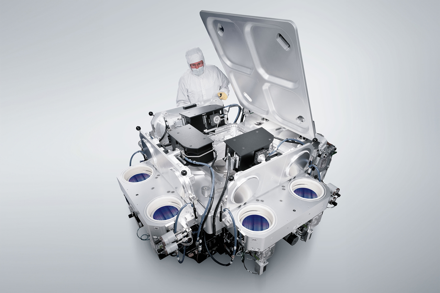
Applied Materials is the world’s largest supplier of equipment for manufacturing semiconductors, displays and other advanced electronics. The company will provide MIT.nano with several state-of-the-art process tools. Specifically, they can support 150 and 200mm wafers and will enhance and upgrade an existing tool owned by MIT. Moreover, Applied engineers will assist MIT.nano in the day-to-day operation and maintenance of the equipment. In addition, they will develop new process capabilities that will benefit researchers and students from MIT and beyond.

“Chips are becoming increasingly complex. There is a tremendous need for continued advancements in 200mm devices, particularly compound semiconductors like silicon carbide and gallium nitride,” said Aninda Moitra, Corporate Vice President and General Manager of Applied Materials’ ICAPS Business.
“Applied is excited to team with MIT.nano to create a unique, open-access site in the U.S. where the chip ecosystem can collaborate to accelerate innovation. Our engagement with MIT expands Applied’s university innovation network. It furthers our efforts to reduce the time and cost of commercializing new technologies. At the same time, it strengthens the pipeline of future semiconductor industry talent.”
Investment from NEMC Hub
Meanwhile, the Northeast Microelectronics Coalition (NEMC) Hub will allocate $7.7 million for the installation of the tools. Specifically, NEMC Hub is managed by the Massachusetts Technology Collaborative (MassTech). It is the regional “hub” that connects and amplifies the capabilities of diverse organizations from across New England, plus New Jersey, and New York. The U.S. Department of Defense (DoD) selected the NEMC Hub as one of eight Microelectronics Commons Hubs. It awarded funding from the CHIPS and Science Act to accelerate the transition of critical microelectronics technologies from lab-to-fab, spur new jobs, expand workforce training opportunities and invest in the region’s advanced manufacturing and technology sectors.
The Office of the Under Secretary of Defense for Research and Engineering (OUSD(R&E)) and the Naval Surface Warfare Center, Crane Division manage the Microelectronics Commons program at the federal level. The National Security Technology Accelerator (NSTXL), which organizes the execution of the eight regional hubs across the country, facilitates it. The announcement for public support was attended by leaders from the DoD and NSTXL.
“The installation and operation of these tools at MIT.nano will have a direct impact on the members of the NEMC Hub, the Massachusetts and Northeast regional economy, and national security. This is what the CHIPS and Science Act is all about,” said Ben Linville-Engler, Deputy Director at the MassTech Collaborative and the interim director of the NEMC Hub. “This is an essential investment by the NEMC Hub to meet the mission of the Microelectronics Commons.”


