ASIA ELECTRONICS INDUSTRYYOUR WINDOW TO SMART MANUFACTURING
Toray Develops New Insulating Resin for Hybrid Bonding
Toray Industries, Inc., has developed an insulating resin material for hybrid bonding (micro bonding). The material is based on Semicofine™ and Photoneece™. These are high-heat-resistant polyimide coatings for semiconductor and display devices. Mainly, the new material combines a conventional polyimide coating agent with the company’s processing and bonding technologies. It can enhance the yields and reliability of semiconductor devices in the hybrid bonding process, which entails bonding semiconductor chips with metal electrodes.
Toray will push ahead with prototyping and providing samples to customers. Mainly, it aims to obtain materials certification in 2025 and start mass production by 2028.
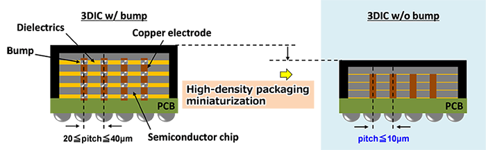
In recent years, the industry has applied three-dimensional (3D) packaging as a leading high-performance packaging technology. This process involves vertically stacking semiconductor chips (Figure 1). Particularly, hybrid bonding is promising for high-performance semiconductor chips requiring fine structures with bump pitches* of 10µ or less. Mainly, Toray markets resin bonding materials for 3D chip-to-chip packaging with fine bump pitches of about 20µ. Hybrid bonding differs from conventional 3D packaging because it entails directly joining metal electrodes without using bumps. Accordingly, this makes it possible to further shorten electrode pitches.
*The spacing between adjacent electrodes joined by solder.
Hybrid Bonding of Semiconductor Packaging
Generally, in hybrid bonding, the chip-to-wafer technique has attracted considerable attention for high-density packaging of different types of chips. This technique involves processing one wafer substrate to the chip size and bonding it to another wafer substrate. Usually, silicon dioxide and other inorganic materials are used as insulating materials for hybrid bonding. However, there are two key challenges with applying the chip-to-wafer technique. First, the silicon dust generated in chip dicing can be trapped during hybrid bonding, causing chip bonding defects and lowering yields. Second, the trapped silicon dust threatens the reliability of semiconductor packages (Figure 2).
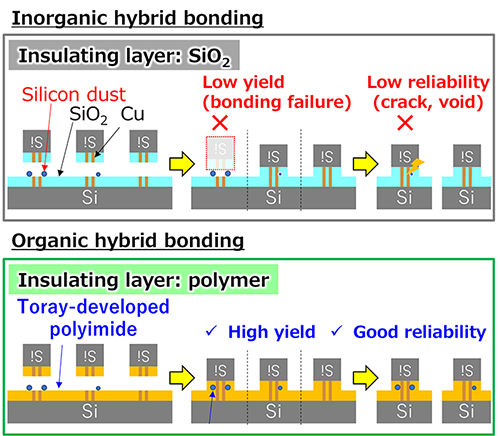
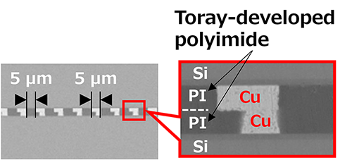
Since 2020, Toray has carried out hybrid bonding experimental demonstrations with the Institute of Microelectronics, a semiconductor research unit of Singapore’s Agency for Science, Technology and Research (STAR). Particularly, this work has tapped the company’s accumulated expertise in functional plastics design technology in employing sophisticated molecular design. Also, it pursued excellence to create insulating polymers offering high heat resistance and excellent mechanical properties (Figure 3). By collaborating with that entity and various semiconductor-related companies, Toray looks to apply this material to chip-to-wafer hybrid bonding. Accordingly, it seeks to boost the yields and reliability of chiplets and make it possible to integrate differing chips in a single package.
Toray will incorporate its new material in its lineup of resin products for semiconductor devices and electronic components to foster the adoption of high-performance next-generation semiconductor packages for high-speed communications devices and server applications. Further, Toray will keep leveraging its core technologies of synthetic organic and polymer chemistry, biotechnology, and nanotechnology. Mainly, it targets the innovation of materials in keeping with its commitment to delivering new value and contributing to social progress.
-21 March 2024-
- Share: