ASIA ELECTRONICS INDUSTRYYOUR WINDOW TO SMART MANUFACTURING
SK hynix Builds New DRAM Fab Amid AI Surge
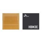
SK hynix Inc. aims to expand production capacity of the next-generation DRAM including High Bandwidth Memory (HBM), a core component of the AI infrastructure. Primarily, this targets the rapidly increasing demand for AI semiconductors.
Following approval by its board of directors, the company will start building the M15X fab in Cheongju, North Chungcheong Province, for the new DRAM production base. It plans to invest about 5.3 trillion won (US$3.9B) for fab construction.
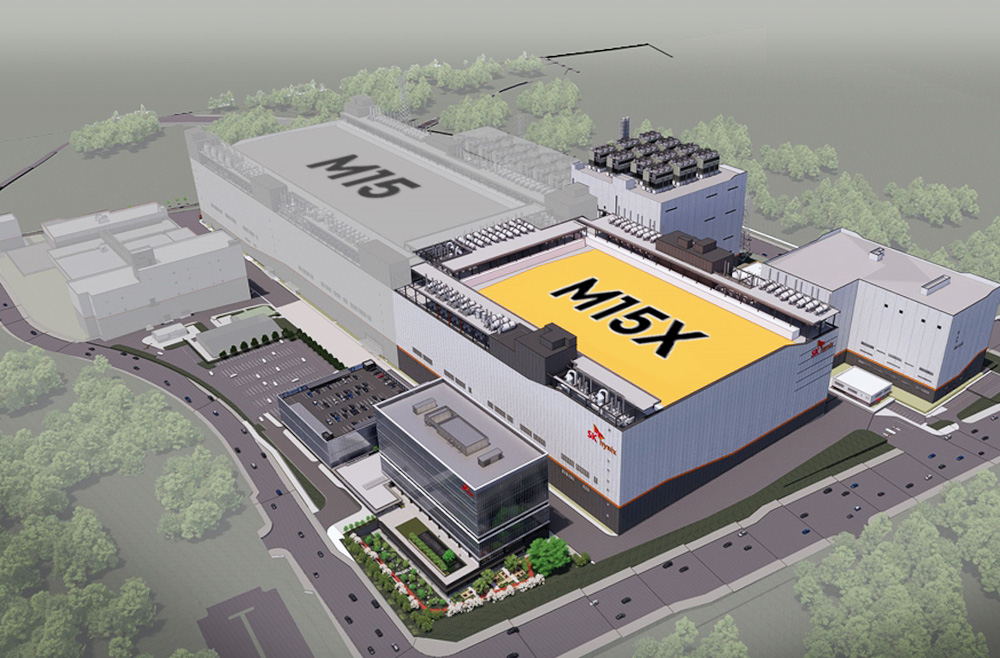
Primarily, SK hynix targets to start construction at the end of April, eyeing completion in Nov. 2025 for an early mass production. As the investment for equipment will gradually increase, the company projects total investments to reach 20 trillion won (US$14.5B) for building the new production base.
As a global leader in AI memory, SK hynix expects the expansion in investment to contribute to revitalizing the domestic economy. At the same time, it will refresh Korea’s reputation as a semiconductor powerhouse.
Ride the Wave of AI Growth
With the advent of AI, the semiconductor industry believes that the DRAM market has entered a mid- to long-term growth phase. Along with HBM, which is expected to grow more than 60% annually, the company forecasts that demand for general DRAM will be on a steady rise. Specifically, high-capacity DDR5 module products for servers will drive this growth.
Moreover, HBM requires at least twice as large capabilities to secure the same production as general DRAM products. Thus, SK hynix believes that increasing DRAM capabilities with a focus on HBM is a precondition for future growth.
Moreover, the company plans to produce new DRAM from the M15X in Cheongju before the completion of the first fab. This is in Yongin Semiconductor Cluster, which is set to begin production in the first half of 2027. Also, M15X is located near M15, which has been expanding Through Silicon Via (TSV)1 capabilities. This makes M15X best conditioned for optimization of HBM production.
1TSV is an interconnect technology. It links upper and lower chips with an electrode that vertically passes through the base logic chip and DRAM chips. There can be thousands of pass-through TSVs depending on the chip design.
-26 April 2024-
- Share: