ASIA ELECTRONICS INDUSTRYYOUR WINDOW TO SMART MANUFACTURING
SK hynix Advances Lead in HBM with TSMC Onboard
SK hynix Inc. has recently signed a memorandum of understanding with TSMC for collaboration to produce next-generation High Bandwidth Memory (HBM). Additionally, it aims to enhance logic and HBM integration through advanced packaging technology. Through this initiative, the company will proceed with the development of HBM4, or the sixth generation of the HBM family. The company plans to mass produce HBM4 starting 2026.
SK hynix said the collaboration with TSMC will lead to more innovations in HBM technology. Also, it will enable breakthroughs in memory performance through trilateral partnership between product design, foundry, and memory providers.
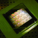
First, the two companies will improve the performance of the base die mounted at the bottom of the HBM package. Particularly, HBM stacks a core DRAM die on top of a base die that features TSV1 technology. Then, a fixed number of layers in the DRAM stack is vertically connected to the core die into an HBM package. The base die located at the bottom connects to the GPU, which controls the HBM.
Technology Collaboration
SK hynix has used a proprietary technology to make base dies up to HBM3E. However, it plans to adopt TSMC’s advanced logic process for HBM4’s base die. This way, packaging additional functionality in a limited space becomes possible. This will help SK hynix produce customized HBM that meets a wide range of demand for performance and power efficiency.
Also, both companies agreed to optimize the integration of SK hynix’s HBM and TSMC’s CoWoS®2 technology. At the same time, they will respond to common customers’ requests related to HBM.
“We expect a strong partnership with TSMC to help accelerate our efforts for open collaboration with our customers and develop the industry’s best-performing HBM4,” said Justin Kim, President and the Head of AI Infra, at SK hynix. “With this cooperation in place, we will strengthen our market leadership as the total AI memory provider further by beefing up competitiveness in the space of the custom memory platform.”
“TSMC and SK hynix have already established a strong partnership over the years. We’ve worked together in integrating the most advanced logic and state-of-the art HBM in providing the world’s leading AI solutions,” said Dr. Kevin Zhang, Senior Vice President of TSMC’s Business Development and Overseas Operations Office, and Deputy Co-Chief Operating Officer. “Looking ahead to the next-generation HBM4, we’re confident that we will continue to work closely in delivering the best-integrated solutions to unlock new AI innovations for our common customers.”
1TSV (Through Silicon Via): An interconnect technology that links upper and lower chips with an electrode that vertically passes through the base logic chip and DRAM chips. There can be thousands of pass-through TSVs depending on the chip design.
2CoWoS (Chip on Wafer on Substrate): A TSMC proprietary packaging process. Mainly, it connects GPU/xPU, a logic chip, and HBM, on a special substrate called an interposer. It is also called 2.5D packaging as the logic chip and the vertically stacked(3D) HBM are integrated into one module which is placed on a horizontal (2D) package substrate.
-19 April 2024-
- Share: