ASIA ELECTRONICS INDUSTRYYOUR WINDOW TO SMART MANUFACTURING
ADEKA Opens New R&D Center in Korea in Advanced ICs
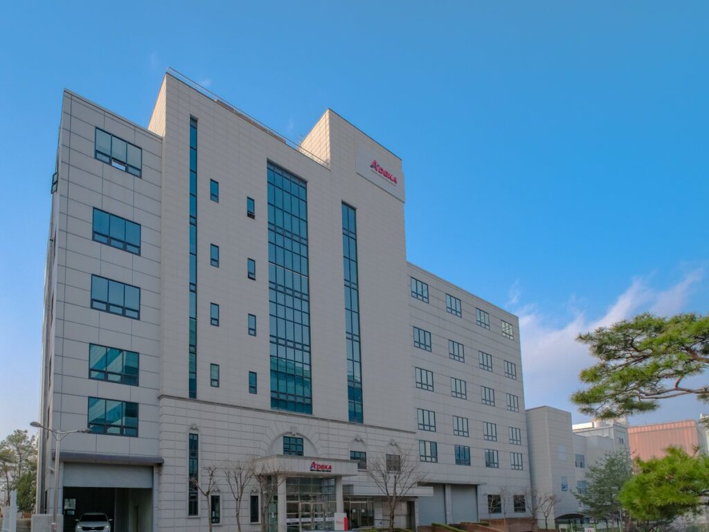
ADEKA KOREA CORPORATION, a consolidated subsidiary of ADEKA, has recently completed its expansion in Korea. Particularly, the expansion involves relocation of its R&D Center and celebrated it with an opening ceremony.
Accordingly, ADEKA put up a new facility to meet the evolving technological innovation in the semiconductor industry. Most importantly, this will further strengthen the group’s position in film deposition evaluation. The company’s objective is to match the same level and development speed with that of semiconductor manufacturers.
Expands Clout in Semiconductor Manufacturing
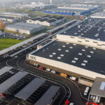
Located in Hwaseong City in Korea’s Gyeonggi Province, ADEKA has acquired the facility with a total floor area seven times larger than the previous one. In addition, the clean room, which is twice the size of the previous one, has expanded the number of ALD deposition and evaluation equipment. Moreover, it will function as a specialty for evaluation and analysis of cutting-edge semiconductor deposition materials.
“We plan to double our equipment and personnel by 2030,” said ADEKA in a statement.
The ADEKA Group’s research and development of new semiconductor materials will continue at Japan’s Oku Central Research Institute in Arakawa-ku, Tokyo.
In early 2026, ADEKA plans to construct and relocate a new research building within the Kuki Area Development Research Institute in Kuki City, Saitama Prefecture. Specifically, this will expand its share of materials for the front-end processes of the group’s main products, semiconductor memory, and logic semiconductors. “We aim to expand our field to include post-process materials,” said ADEKA.
The ADEKA Group aims to become the world’s top semiconductor materials manufacturer by building a strong system in major semiconductor manufacturing areas around the world.
Advanced IC Material Plant in Korea
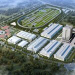
Early this year, ADEKA said it will construct a new manufacturing building inside its 3rd Jeonju Plant of ADEKA Korea Corporation. Particularly, the new plant will provide the company with a space for a mass production system of new materials for next-generation semiconductors.
Semiconductors are essential to realizing an advanced ICT society that harnesses megatrends such as 5G communications and AI. Thus, semiconductors are becoming more highly integrated due to miniaturization, faster information processing, and lower power consumption. For that reason, semiconductors need advanced materials to support demands.
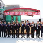
In the ADEKA Group’s medium-term management plan ADX 2023 (FY2021-2023), the “next-generation ICT field” is one of the important fields. Hence, ADEKA is actively investing in cutting-edge semiconductor materials. Particularly, the company is actively investing in cutting-edge semiconductor materials. At the same time, it is also building up research and development and a production system in Taiwan.
Moreover, ADEKA KOREA is actively making capital investments to increase production. In addition, it is also expanding its product lineup of the ADEKA Orcera series, a high dielectric material for cutting-edge semiconductor memory. Currently, it has the world’s No. 1 market share *.
The planned manufacturing building will enable ADEKA to set up a production system in a short time. Also, this will ensure a stable supply of materials for next-generation devices for mass production.
The company will construct the new building at its third factory in Jeonju, which it acquired in 2022.
21 May 2024
- Share: