ASIA ELECTRONICS INDUSTRYYOUR WINDOW TO SMART MANUFACTURING
Applied Materials to Offer New Approach in Chip Wiring
Applied Materials, Inc. has introduced materials engineering innovations designed to increase the performance-per-watt of computer systems. Specifically, by enabling copper wiring to scale to the 2nm logic node and beyond.
“The AI era needs more energy-efficient computing, and chip wiring and stacking are critical to performance and power consumption,” said Dr. Prabu Raja, President of the Semiconductor Products Group at Applied Materials.
In addition, Dr. Raja said, “Applied’s newest integrated materials solution enables the industry to scale low-resistance copper wiring to the emerging angstrom nodes, while our latest low-k dielectric material simultaneously reduces capacitance and strengthens chips to take 3D stacking to new heights.”
Overcoming the Physics Challenges of Classic Moore’s Law Scaling
Today’s most advanced logic chips can contain tens of billions of transistors connected by more than 60 miles of microscopic copper wiring. Moreover, each layer of a chip’s wiring begins with a thin film of dielectric material. The etching process enables this material to create channels that are filled with copper. For decades, low-k dielectrics and copper have been the industry’s workhorse wiring combination. Thus, allowing chipmakers to deliver improvements in scaling, performance, and power efficiency with each generation.
However, as the industry scales to 2nm and below, thinner dielectric material renders chips mechanically weaker, and narrowing the copper wires creates steep increases in electrical resistance that can reduce chip performance and increase power consumption.
Enhanced Low-k Dielectric Reduces Interconnect Resistance and Strengthens Chips for 3D Stacking
Applied’s Black Diamond™ material has led the industry for decades. This is surrounding copper wires with a low-dielectric-constant – or “k-value”. The film engineered to reduce the buildup of electrical charges that increase power consumption and cause interference between electrical signals.
Furthermore, Applied has introduced an enhanced version of Black Diamond, the latest in the company’s Producer™ Black Diamond™ PECVD* family. This new material reduces the minimum k-value to enable scaling to 2nm and below. Moreover, while offering increased mechanical strength which is becoming critical as chipmakers and systems companies take 3D logic and memory stacking to new heights.
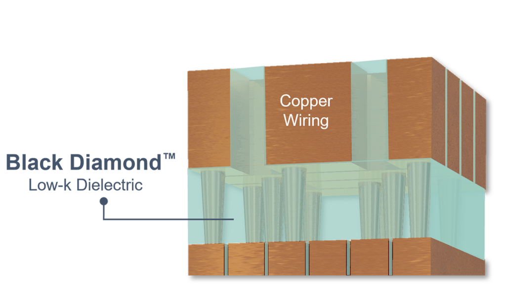
The latest Black Diamond technology is being adopted by all leading logic and DRAM chipmakers.
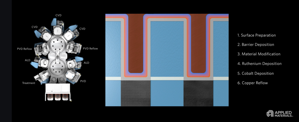
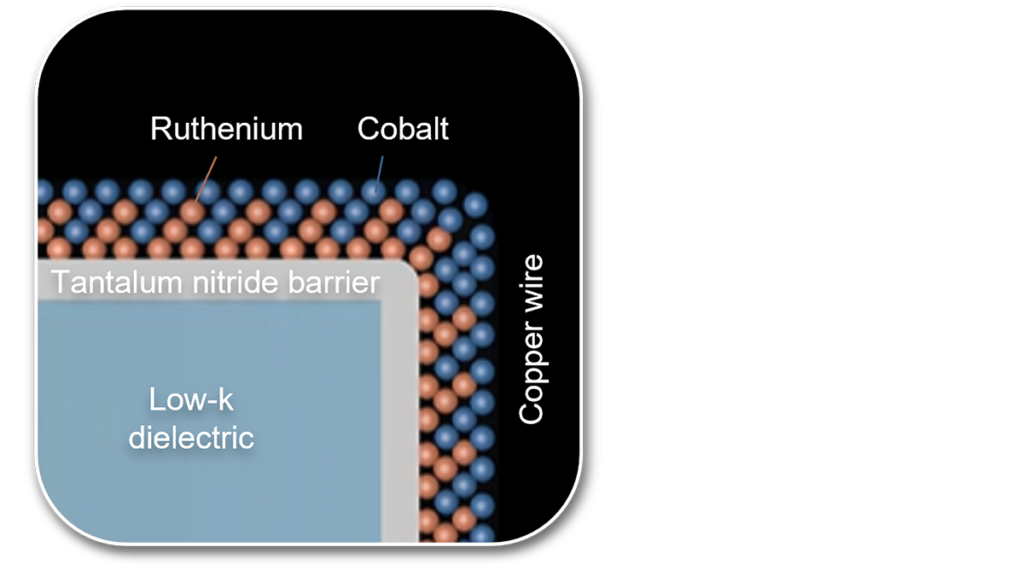
New Binary Metal Liner Enables Ultrathin Copper Wires
To scale chip wiring, chipmakers etch each layer of low-k film to create trenches, then deposit a barrier layer that prevents copper from migrating into the chip and creating yield issues.
The barrier is then coated with a liner that ensures adhesion during the final copper reflow deposition sequence, which slowly fills the remaining volume with copper.
As chipmakers further scale the wiring, the barrier, and liner take up a larger percentage of the volume intended for wiring, and it becomes physically impossible to create low-resistance, void-free copper wiring in the remaining space.
Today, Applied Materials publicly introduced its latest IMS™ (Integrated Materials Solution™) which combines six different technologies in one high-vacuum system, including an industry-first combination of materials that enables chipmakers to scale copper wiring to the 2nm node and beyond. The solution is a binary metal combination of ruthenium and cobalt (RuCo), which simultaneously reduces the thickness of the liner by 33 percent to 2nm, produces better surface properties for void-free copper reflow, and reduces electrical line resistance by up to 25 percent to improve chip performance and power consumption.
The new Applied Endura™ Copper Barrier Seed IMS™ with Volta™ Ruthenium CVD* is being adopted by all leading logic chipmakers and began shipping to customers at the 3nm node. An animation of the technology can be viewed here.
09 July 2024
- Share: