ASIA ELECTRONICS INDUSTRYYOUR WINDOW TO SMART MANUFACTURING
Rapidus to Soar 2nm With Japan's First EUV Line
Rapidus Corporation said it has delivered and started the installation of an EUV exposure tool manufactured by ASML of the Netherlands. Accordingly, Rapidus will install the latest equipment at its Innovative Integration for Manufacturing (IIM), which are currently under construction in Chitose City in Japan’s Hokkaido.
To commemorate this, the company held a ceremony at Portom Hall in New Chitose Airport.
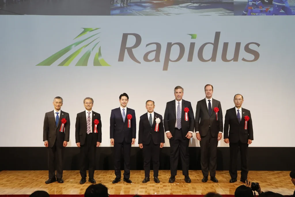
Japan’s First EUV Tool
As a result, the installation of the EUV exposure tool, which is compatible with mass production of cutting-edge semiconductors, is the first time in Japan. In addition, several other semiconductor manufacturing equipment and transport systems are also up for installation in the future at Rapidus’ IIM-1. Thus, helping the company realize the production of 2nm generation semiconductors.y
EUV lithography is one of the key technologies for realizing 2nm generation semiconductors. In particular, the lithography process is a key process for forming the 2nm generation gate-all-around (GAA) structure.
Before 2nm, ArF (193nm) immersion exposure technology was at the forefront in manufacturing processes. However, short wavelengths using EUV (13.5nm) will be essential for the 2nm generation and beyond.
Moreover, EUV lithography technology will use light sources, optical systems, and photomasks that are different from those used up until now. The EUV exposure equipment from ASML that will be introduced this time uses an optical system that uses a reflective photomask and mirror lenses.
It adopts the TWINSCAN platform, which performs alignment and scanning on separate stages. Furthermore, it also realizes increased productivity while responding to miniaturization.
Rapidus will introduce a pilot line operation at IIM-1 in April 2025. Single-wafer processing will also happen for all manufacturing equipment. Thus, the company will proceed with the establishment of a new semiconductor foundry service, Rapid and Unified Manufacturing Service (RUMS).
19 December 2024
