ASIA ELECTRONICS INDUSTRYYOUR WINDOW TO SMART MANUFACTURING
Amkor Breaks Ground on New Chip Packaging, Test Line
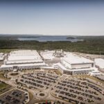
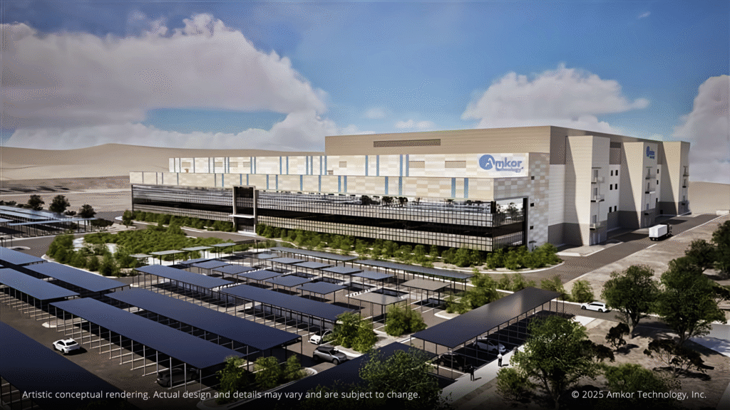
Chip packaging and test services provider Amkor Technology, Inc. has broken the ground for its latest investment at its new state-of-the-art outsourced semiconductor advanced packaging and test campus in Arizona.
The expanded investment includes additional cleanroom space and a second greenfield packaging and test facility. Accordingly, this will increase total project investments, totaling US$7 billion, across two phases.
The company held a groundbreaking ceremony on Oct. 6 (GMT -7, Arizona, United States) that brought together government officials and other industry stakeholders. Amkor’s investment supports the broader strategy to strengthen U.S. semiconductor leadership and will be the first U.S. based high volume advanced packaging facility.
Apex of United States’ Advanced Packaging Grit
The campus will offer over 750,000 square feet of cleanroom space and as many as 3,000 high-quality jobs once it concludes construction in mid-2027. Actual production will start early 2028.
The new greenfield facilities will serve as a cornerstone of United States’ advanced packaging capabilities, supporting key customers including Apple and NVIDIA. Amkor’s expanded investment got the support of U.S. government’s various semiconductor and manufacturing programs.
“This groundbreaking represents a bold step in Amkor’s long-term strategy for growth and innovation,” said Giel Rutten, Amkor’s president and chief executive officer. “We’re building a facility to meet our customers’ most advanced needs that will help shape the future of semiconductor manufacturing in the United States. Arizona offers the right mix of talent, infrastructure, and industry presence, and we’re proud to deepen our roots here.”
State-of-the-Art Facilities
The Amkor facility is located in the northern part of Peoria, the city is Arizona’s growing high-tech corridor. The campus will house the most sophisticated outsourced semiconductor packaging and test facilities in the country.
In addition, the facility will feature smart factory technologies and scalable production lines to meet evolving market demands for AI, high performance computing, mobile communications, and automotive applications.
Furthermore, the campus will focus on advanced packaging and testing technologies and will complement TSMC’s front-end wafer fabrication for full end-to-end semiconductor manufacturing.
07 October 2025
- Share: