ASIA ELECTRONICS INDUSTRYYOUR WINDOW TO SMART MANUFACTURING
New SMT Trends Propel Full Automation of Factories
Surface mount technology (SMT) continues to evolve targeting high-quality manufacturing. For example, it is already common nowadays to monitor operation conditions of SMT lines in overseas plants from remote locations, for example in Japan. The realization of unmanned fully automated production plants is right around the corner.
Manufacturing in Japan faces various issues, including the decreasing working population and succession of skilled engineers. A recent population forecast of United Nations said China, which houses many factories, will become a super-aged society by 2035. Therefore, the ratio of 65 and older people will reach 21 percent. This means, the decrease in the labor population will increase the severity of issues involving manufacturing.

In addition, the coronavirus (COVID-19) pandemic caused the closure of several plants in China and various parts of the world. Hence, this puts to question current states of business continuity plans (BCP) and supply chains. To prevent the expansion of infections through people, interest in the automation of production through robots and smart factories, as well as in fully automated plants and unmanned plants has increased.
Because of these, smart factories that significantly improve productivity using internet of things (IoT) technology have been attracting attention worldwide. As such, huge manufacturers have led the drive to smarter factories. Now, the momentum is spreading to small and medium-sized plants as well.
Use IoT, AI
Manufacturers of mounters and mounter-related products have been promoting smart factories globally, while expanding collaborations with other companies. In smart factories, mounters aim to achieve high-quality production through self-contained manufacture without human intervention. Consequently, this combines IoT and artificial intelligence (AI) technologies and by connecting machines for exchanging digital data among them.
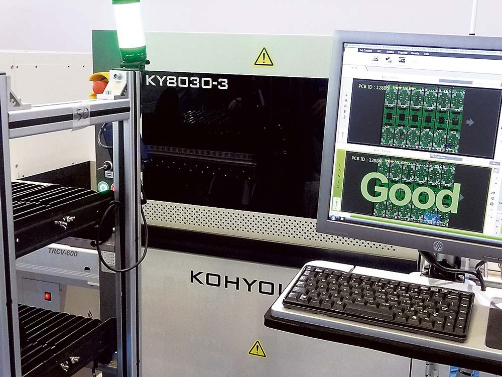
For example, an inspection system at the final process of the SMT process for PCBs can detect a defect, such as a missing part. As such, the inspection system sends the information to the mounter, which automatically corrects the failure and eliminates the production of defective products.
Adoption of IoT in production will visualize production equipment. In addition, methods to realize visualization of machine element components, such as bearings and linear motion guides in various production equipment, have started to expand. Sensing vibrations and sounds of linear motion guides and digitizing collected data enable the analyses of subtle changes in vibrations and abnormal noises and prediction of machine failure. It is also possible to check the timing of maintenance.
Meanwhile, introducing IoT and making the entire production line or entire factory smart requires huge costs. Therefore, systems that read the pointers of existing analog instruments in the factory using a camera and a sensor and digitize the figures for remote monitoring via cloud have also been commercialized.
PCB Inspection Systems
Manufacturers of inspection systems for printed circuit boards (PCBs) have been striving to expand business. As a result, they implement a wide range of strategies, from introducing new products, expansion of functions, and creation of new fields.
Moreover, there have been higher integration of PCBs, and the spread of contactless works and automation amid the COVID-19 pandemic. These factors have contributed to the increased demand for PCB inspection systems. Conventionally, PCBs in the mounting process have been visually inspected by people. However, components to be mounted have become smaller, and wirings have become finer. Thus, PCBs with higher densities have made manual visual inspection difficult, and labor costs have also increased, making PCB inspection systems indispensable.
PCB inspection systems may come as solder paste inspection (SPI) systems, automated optical inspection (AOI) systems, and automated X-ray inspection (AXI) systems. Recently, three-dimensional (3D) inspection systems that perform precise inspections by adding height inspection to plane inspection have become the mainstream.
Soldering Technologies
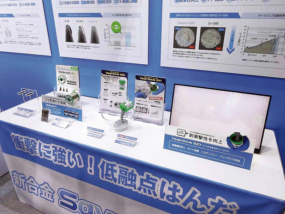
Meanwhile, soldering continues to evolve. As a result, manufacturers race to develop solder products that solve various technological challenges and meet carbon neutral requirements.
These technological challenges include low-temperature solders, and high-strength solders for PCBs for automotive devices. The need to reduce voids, use of multiple elements to cope with rising tin (Sn) and silver (Ag) prices, are also part of the challenge. Moreover, manufacturers also need to address compatibility with automatic machines (soldering robots), and the DIP soldering method.
The joining process in soldering is possible through wetting, melting, and spreading of the base metal and solder after the removal of oxidized film due to flux. Particularly, wettability affects the functionality and safety of products. Hence, this becomes an indispensable characteristic in soldering.
Interest in carbon neutrality has been surely increasing, and solders with low melting points have been attracting attention. Low melting points of solders have good effects to various processes in soldering, including the simplification of the mounting process, not limited to power saving of the soldering chamber. As a result, it leads to carbon neutrality.
End-consumer products continue to diversify. Specifically, this is true for smartphones and electric vehicles (EVs). Hence, commercialization of solders that meet changing product demands continues. This include solders with increased joining strength with the addition of indium (In), cobalt (Co), antimony (Sb), and germanium (Ge).
Another important challenge in soldering is the suppression of a phenomenon called void. Voids are bubbles that generate in solders and become a cause of defects. Various measures have been taken to suppress voids that generate when solder melts and hardens. Vacuum reflow ovens also attract attention as equipment that contributes to the reduction of voids. They suppress the generation of voids that generate in solder joints by providing a vacuum zone in the solder bath.
- Share: