ASIA ELECTRONICS INDUSTRYYOUR WINDOW TO SMART MANUFACTURING
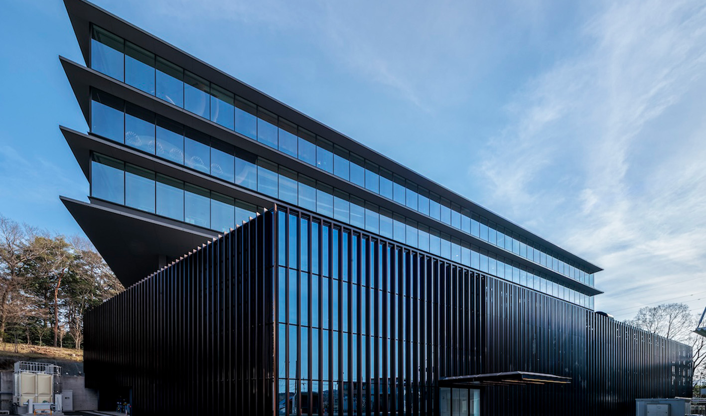
Taiyo Ink Opens New Technology Center in Japan
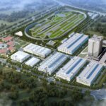
Taiyo Ink Mfg. Co., Ltd., an electronics subsidiary of Taiyo Holdings Co., Ltd., opened a new technology development center, InnoValley, in April in Japan.
The opening of InnoValley represents an investment in human capital to develop autonomous human resources. Also, it aims to strengthen global technology development capabilities for semiconductor-related materials and other products.
Taiyo Holdings is a global manufacturer of solder resist, an insulating material that protects the surface of printed circuit boards.
Meanwhile, Taiyo Ink Mfg. is responsible for the development, manufacture, sale, and purchase of chemical products for electronic equipment, including solder resist and other components for printed circuit boards in the electronics business.
Enhance Corporate Value
Primarily, InnoValley is Taiyo Holdings Group’s first technology development center.
Giving a background for the opening of the technology center, Eiji Sato, President of Taiyo Holdings, said, “Both the group’s electronics business sales and the number of employees at Taiyo Ink Mfg. have doubled in the past decade. We opened this facility to put the business on a further growth trajectory in line with the recovery of the semiconductor market. (Also, we aim) to enhance corporate value by realizing human capital management.”
President Shoji Minegishi of Taiyo Ink Mfg. said, “The Technology Development Center is an important facility for accomplishing our electronics business strategies. Specifically, they are 1) strengthening the solder resist customer base; 2) creating new business development; 3) speeding up the continuous launch of new products; and 4) creating new applications. As a leading solder resist company, we would like to contribute to Japan’s manufacturing industry.”
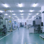
The technology development center is a six-storey building with a total floor area of approximately 10,400sqm. Primarily, it was designed to maximize the potential of employees by creating different environments: a laboratory area on the lower floors (1-3F) and an office area on the upper floors (4-6F).
This is an English translation of an original Japanese article published in Dempa Shimbun Daily.
-22 May 2024-
- Share: