ASIA ELECTRONICS INDUSTRYYOUR WINDOW TO SMART MANUFACTURING
EDP Adds New Low-Resistance Diamond Substrate
EDP Corporation, a Japanese manufacturer of synthetic diamonds, has announced that it increased the size of the low-resistance substrates released last year and now, is introducing it as a new product. Primarily, the new product has a size of up to 13×13mm.
Specifically, the “Large Low Resistance PCB” features self-supporting single-crystal substrate containing high concentration of boron (boron) impurities and high conductivity.
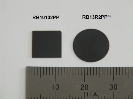
RB10102PP: Low resistance PCB 10×10×0.2mm double-sided polishing
RB13R2PP**: Low Resistance Minimal Wafer
Uses Synthetic Diamond as Semiconductor Material
Mainly, EDP has been selling various substrates for research and development that use diamond as a semiconductor material. Specifically, in August last year, the company commercialized a substrate with a low resistance value and an epitaxial substrate doped with a high concentration of boron.
Generally, diamond is expected to be applied as a semiconductor material for power devices that control large amounts of power in electric vehicles and other vehicles. For such a device to carry a large current, it is necessary to have a vertical device structure in which the current flows between the top and bottom of the device. Thus, to realize this structure, the wafers and substrates that form the devices must be highly conductive.
Normally, diamond is electrically insulating, but it is known that high concentrations of boron can make it electrically conductive. EDP has succeeded in producing a single-diamond crystal containing a high concentration of boron by mixing a large amount of boron raw material into the reaction gas of gas-phase deposition. As a result, it has commercialized both a free-standing substrate and an epitaxial substrate grown on a normal substrate.
However, the size of the free-standing board was limited to 7×7mm or less. Also, it was not possible to support the research and development of large devices that carry large currents or the production of a large number of devices on a single board. Therefore, EDP has expanded the area of low-resistance substrates by using large single crystals such as 15x15mm, which was released in November last year.
As a result, it has succeeded in developing a self-supporting single crystal substrate up to 13×13mm, which is now being released as a new product. The boron concentration and resistance values contained are the same as those of low-resistance substrates that have been sold for a long time.
Product Contents and Properties:
Large high boron-concentration diamond products have the following specifications:
- Boron concentration: 2×10²⁰~4×10²⁰/cm3
- Resistance: 20mΩcm or less
- Shape specification: 13x13mm or less (round wafers can also be manufactured)
- Thickness: 0.1~0.2mm range. The thickness accuracy is -0, +0.05mm azimuth :(100), and there is an off-angle of about 3° on the face.
- Surface condition: Double-sided polishing (Ra<5nm or <2nm)
Impact on Business Results
The development of diamond devices is currently in the basic research stage. However, the substrates used for this are expected to steadily form a market in the near future. This fiscal year, EDP expects that sales of this product will be about 150 units of the small self-supporting low-resistance substrate and the low-resistance epitaxial substrate that it has been selling so far. “We do not believe that this will have a significant impact on our business performance,” according to EDP.
However, since the development of diamond power devices is expected to intensify from the next fiscal year, EDP will consider increasing production capacity depending on market conditions.
This is an online translation of a Japanese press release with slight editing made by Dempa.
-27 September 2024-
- Share: