ASIA ELECTRONICS INDUSTRYYOUR WINDOW TO SMART MANUFACTURING
New Nikon UV Camera Lens Zooms in on IC Wafer
Nikon Corporation has released the new C-mount industrial lens Rayfact UV25mm F2.8, designed for use with ultraviolet cameras. Primarily, this Rayfact UV lens series is ideal for visual inspections of semiconductor wafers and electronic components. Mainly, it detects microscopic scratches and surface irregularities. Also, it can identify materials that are difficult to distinguish under visible light. Additionally, this lens series is used in areas such as combustion and plasma research and its applications are expected to expand in the future.
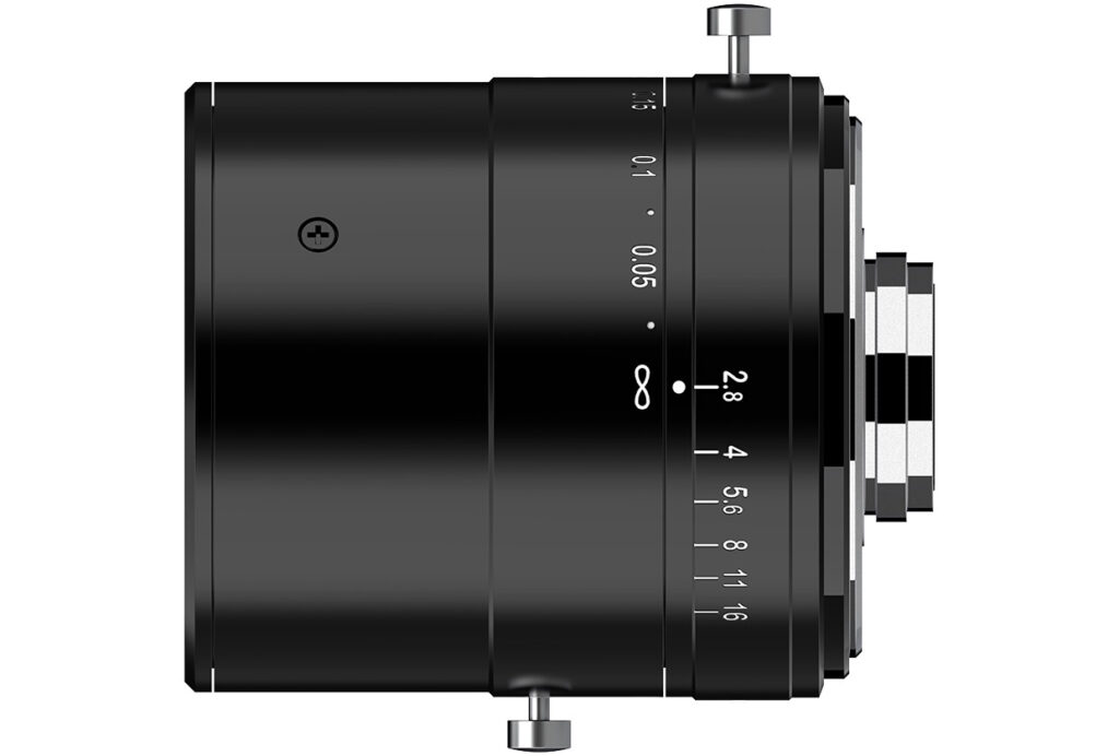
Particularly, the Rayfact UV25mm F2.8 is optimized for use with the IMX487 high resolution UV image sensor featuring the industry’s smallest* 2.74µm square pixels manufactured by Sony Semiconductor Solutions Corporation. This lens is designed to ensure clear images all the way to the edges. Moreover, it is brighter compared to previous products. Thus, it enables high resolution inspections over lager areas.
*As of October 21, 2024, according to a survey by Nikon Corporation
-21 October 2024-
- Share: