ASIA ELECTRONICS INDUSTRYYOUR WINDOW TO SMART MANUFACTURING
Tokyo Electron Completes New Building in Miyagi
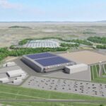
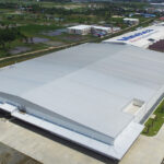
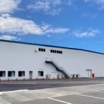
Tokyo Electron has announced that its development and manufacturing subsidiary, Tokyo Electron Miyagi (Taiwa-cho, Miyagi), has completed its new development building (Development Building No. 3). The company held completion ceremony Thursday (Apr. 24).
As the transition to a digital society accelerates, the demand for semiconductors is likely to grow significantly. Thus, the increasing complexity and diversity of semiconductors, along with finer line widths of chips, patterning technologies critical to semiconductor innovation continue to evolve.
-1024x618.jpg)
Moreover, the market for etch systems developed and manufactured by Tokyo Electron Miyagi will expand even further.
Offers Complete System Solutions
The new development building prioritizes safety, quality, and environmental considerations. At the same it enables sophisticated and efficient development operations through advanced digital technologies.
既存棟_宮城技術革新センター外観(東京エレクトロン宮城)-1024x768.jpeg)
Enhancing the timely delivery of the high value-added, high quality products that customers need, TEL will contribute to the sustainable medium- to long-term corporate growth and the progress of society.
In keeping with the motto of Best Products and Best Technical Service, TEL aims to work with its customers to pursue semiconductor technology innovations. These innovations have been essential to achieving both digitalization and decarbonization.
TEL is the only semiconductor production equipment manufacturer in the world to offer system solutions for all four sequential patterning processes: deposition, coating/development, etch, and cleaning.
The new development building in 1 Techno-Hills in Miyagi’s Taiwa-cho, Kurokawa-gun, spans total floor area of 46,000sq.m, excluding the ancillary facility area.
The three-story, 52-billion-yen facility, will develop semiconductor manufacturing equipment including plasma etch systems.
25 April 2025
- Share: