ASIA ELECTRONICS INDUSTRYYOUR WINDOW TO SMART MANUFACTURING
TSMC’s New 1.4nm Tech Process to Start 2028
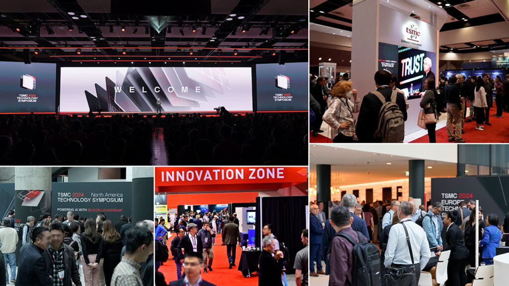
TSMC has announced its next cutting-edge logic process technology, A14 (1.4nm), at the company’s North America Technology Symposium. Accordingly, the forthcoming 1.4nm-class technology will make significant advancements from the N2 (or 2nm) process.
TSMC Chairman and CEO Dr. C.C. Wei said the A14 will form part of the company’s cutting-edge solutions that will connect physical and digital worlds amid the advancement of AI.
“Our customers constantly look to the future, and TSMC’s technology leadership and manufacturing excellence provides them with a dependable roadmap for their innovations,” said Wei.
In addition, Wei said, “TSMC’s cutting-edge logic technologies like A14 are part of a comprehensive suite of solutions that connect the physical and digital worlds to unleash our customers’ innovation for advancing the AI future.”
Improves On-Board AI Functions of Devices
The A14, which the company said will enter production in 2028, will offer significant advancement from TSMC’s industry-leading N2 process. It was only in 2022 the company announced N2 process, which will go on volume production later this year (2025).
Accordingly, the company designed the new A14 class technology to drive AI transformation further as it promises to deliver faster computing and greater power efficiency.
Moreover, the novel process technology will definitely bring about significant enhancements to chips for smartphones. Specifically, it will improve the on-board AI capabilities, making them even smarter. TSMC said the current A14 development is progressing smoothly with yield performance ahead of schedule.
Compared with the N2 process, the A14 will offer up to 15 percent speed improvement at the same power, or up to 30% power reduction at the same speed, along with more than 20% increase in logic density. Leveraging the Company’s experience in design-technology co-optimization for nanosheet transistor, TSMC is also evolving its TSMC NanoFlex™ standard cell architecture to NanoFlex™ Pro, enabling greater performance, power efficiency and design flexibility.
What Does 1.4nm Process Brings
The announcement of 2nm process technology has already brought about unprecedented performance and efficiency, making it another breakthrough leap in semiconductor manufacturing.
Therefore, the announcement of the next-generation 1.4nm process technology of producing chips will enable TSMC to bring about sophisticated innovations across broad range of sectors. This is because the new technology will push further he limits of what chips can do to enable more powerful and efficient performance in computing, AI, and IoT applications.
Basically, paving the way of 1.4nm semiconductor manufacturing process will enable a higher density transistors on a chip compared to earlier nodes such as 2nm. The manufacturing process, that is 1.4nm, will able to pack more transistors onto a chip as it will take miniaturization way further than it did in 2nm.
Because of these, chips that will come out of the 1.4nm process will more than likely consume less power and offer higher performance. Thus, making the technology more suitable for mobile devices and edge computing where batter life and thermal management will play important roles.
Other Announcements
In addition to A14, TSMC also debuted new logic, specialty, advanced packaging and 3D chip stacking technologies at TSMC’s North America Technology Symposium. Therefore, each contributing to broad technology platforms in High Performance Computing (HPC), smartphone, automotive, and Internet of Things (IoT). These offerings aim to equip customers with a comprehensive suite of interconnected technologies to drive their product innovations. Among them are as follows:
High Performance Computing
TSMC continues to advance its Chip on Wafer on Substrate (CoWoS) technology to address AI’s insatiable need for more logic and high-bandwidth memory (HBM). Thus, the company plans to bring 9.5 reticle size CoWoS to volume production in 2027. This will enable integration of 12 HBM stacks or more in a package together with TSMC’s leading-edge logic technology.
Smartphone
As TSMC supports AI on edge devices even further, there also rise the need for high-speed, low-latency wireless connectivity. To make this happen, the company introduced N4C RF, the latest generation of TSMC’s radio frequency technology.
N4C RF delivers 30% power and area reduction versus N6RF+, making it ideal for packing more digital content into RF system-on-chip designs to meet the requirements of emerging standards such as WiFi8 and AI-rich True Wireless Stereo. TSMC scheduled it to enter risk production in first quarter of 2026.
Automotive
Advanced Driver Assistance Systems (ADAS) and Autonomous Vehicles (AV) pose stringent demands for computing power with no compromise on automotive-grade quality and reliability. Therefore, TSMC is meeting customers’ needs with the most advanced N3A process going through the final stage of AEC-Q100 Grade-1 qualification, and continuous defect improvement to meet Automotive defective parts per million (DPPM) requirements. N3A is entering production for automotive applications, joining a full suite of technologies for future software-defined vehicles.
Internet of Things
With TSMC’s previously announced ultra-low power N6e process now in production, the company is targeting N4e to continue pushing the envelope of power efficiency for future edge AIs.
24 April 2025
- Share: