ASIA ELECTRONICS INDUSTRYYOUR WINDOW TO SMART MANUFACTURING
LG Innotek Unveils New Chip Substrate Tech for Mobiles
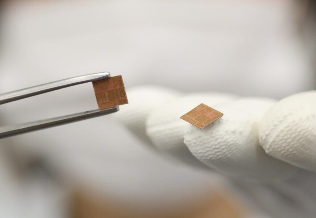
LG Innotek said it has developed a next-generation copper post (Cu-Post) technology as a high-value-added semiconductor substrates for mobile devices.
Accordingly, the first copper post technology will enable denser circuitry for smaller, higher-performance semiconductor substrates with improved heat dissipation. This, LG Innotek said, “will change the industry paradigm” as the company seeks to grow its semiconductor parts business with a target annual revenue of US$2.2 billion by 2030.
Development Background
Over the years, manufacturers of mobile devices have been seeking ways to reduce the size of smartphones. In fact, demand is soaring for mobile device semiconductor substrates, such as the Radio Frequency-System in Package (RF-SiP), that provide maximum performance in a minimal size.
Because of this trend, LG Innotek started in 2021 the development of its Cu-Post technology, which uses a copper post to connect a semiconductor substrate and mainboard.
Most importantly, this groundbreaking technology allows the semiconductor substrates to hold more circuits and increases the semiconductor package’s ability to release heat. LG Innotek said the copper post technology will enable them to solidify further its leadership in the global RF-SiP substrate market.
Role of Semiconductor Substrate
A semiconductor substrate connects electronic components such as semiconductor chips, power amplifiers, and filters, to a mainboard. The semiconductor substrates are connected to a mainboard through solder balls that allow the exchange of electrical signals. The denser the arrangement of solder balls, the more circuits can be connected implemented, which is a core requirement for improving smartphone performance.
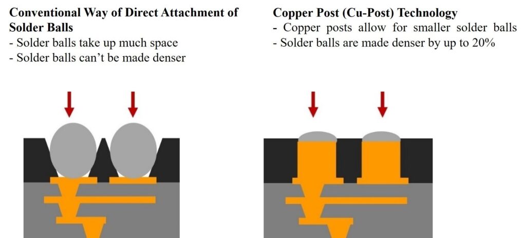
Conventionally, solder balls were attached directly to the semiconductor substrate to connect to the mainboard. The solder balls need to be sufficient in size with ample spacing to ensure stable connection. However, this method prevents a denser arrangement of solder balls, which would allow higher circuit count (see Figure 1, left image).
Because of this LG Innotek deviated from the conventional method and instead used smaller solder balls mounted on top of copper posts attached to the semiconductor substrate (see Figure 1, right image).
Suits AI, Other Smartphone Trends
With the Cu-Post technology, LG Innotek can squeeze almost 20% more solder balls onto the semiconductor substrate. The technology minimizes the area and size of the solder balls thus allows the denser layout of solder balls, as the posts, made of copper with a high melting point, retain their form at high heat.
According to LG Innotek, the Cu-Post technology is optimized for high-performance smartphones designed for AI computations, which require efficient processing of large volumes of complex electrical signals.
For the same-sized semiconductor substrate, the Cu-Post technology allows it to accommodate more solder balls and circuits, with denser circuitry being required for high-performance semiconductor substrates.
Moreover, the said technology also improves smartphones’ ability to dissipate heat as Cu has seven times higher thermal conductivity than the traditional solder (Pb). Because of this, Cu-Post technology enables stable mobile device performance as it can minimize heat-related issues, such as reduced chip performance and signal loss.
07 July 2025
- Share: