ASIA ELECTRONICS INDUSTRYYOUR WINDOW TO SMART MANUFACTURING
ASMPT’s New Tool to Soar Chip Bonding to New High
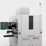
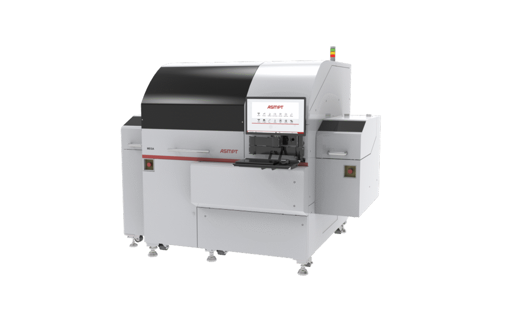
Advanced packaging and semiconductor assembly solutions provider ASMPT Semiconductor Solutions (ASMPT SEMI) has introduced its new MEGA multi-chip bonding platform, which the company said sets the standard in precision and speed with.
High flexibility, a modular structure, and low space requirements are among the innate characteristics of the new device family. With 12k UPH, the MEGA-G version is designed for maximum speed. With the MEGA-P and its unprecedented precision of ±2 µm, ASMPT SEMI targets primarily photonics manufacturers.
Meets Demand for Next-Gen Servers, AI EDGE, ADAS
Specifically, a multi-chip bonding platform plays crucial role for the production of advanced semiconductor packages. This technology integrates multiple chips into a single package. Therefore, offering a high-precision solution for the diverse needs of modern electronics.
The MEGA platform offers various epoxy dispensing and stamping functions as well as the ability to use multiple adhesives side-by-side while monitoring their application with a 3D inspection system. Even immediate fixation via UV curing is available. The picking and bonding arms operate independently of each other, with a flip-pick arm and a rotation unit for precise alignment located between them.
As a die bonder for high-performance computer chips, the MEGA perfectly meets the requirements for the next generation of server clusters and AI edge devices such as smartphones and advanced driver assistance systems (ADAS), as well as data and telecommunication applications.
Highly Flexible Feeding Options
With its automatic bonding tool change capability, up to ten bonding tool buffers and five ejection tools, this extraordinarily versatile machine quickly adapts to new tasks. The ASMPT SEMI’s MEGA platform is also highly flexible with regard to its wafer supply and the way it handles dies and substrates. For example, dies can be supplied via waffle packs, Gel-Paks, or an optional tape feeder station.
The multi-chip bonder processes wafers with diameters of up to 12 inches and dies measuring 0.15 × 0.15 mm to 10 × 10 mm, as well as substrates measuring up to 130 × 300 mm.
The MEGA’s customizable options meet the packaging requirements of sophisticated multi-chip components and make it the bonder of choice for optical transceivers, photonics, sensors, and other highly advanced applications. To accomplish this, the MEGA-P model uses a patented high-precision bonding head with integrated optics that achieves a placement accuracy of ±2 µm and ±0.1 degrees.
“The MEGA multi-chip bonder performs, in a single machine, tasks that used to require a whole line of machines,” explains Dr. Johann Weinhändler, Regional Head ASMPT Semiconductor Solutions Europe and CEO of ASMPT AMICRA in Regensburg, Germany. “We have made sure that chip manufacturers still retain maximum flexibility. The machine’s modular structure also makes it customizable to the user’s specific needs, ensuring that one does not have to pay for functions that are not needed.”
14 August 2025
- Share: