ASIA ELECTRONICS INDUSTRYYOUR WINDOW TO SMART MANUFACTURING
New OKI Tech Allows Optical Devices Mounting on 300mm
Oki Electric Industry Co., Ltd. has developed tiling crystal film bonding (CFB) technology that enables heterogeneous integration of small-diameter optical semiconductor wafers on 300mm silicon wafers.
Previously, such process was not possible due to wafer size restrictions. OKI expects this will further advance photonics and electronics convergence.
Overcomes Disparity in Wafer Sizes
Recently, rapid advances in AI has fueled growing demand for power-hungry data centers. Applying photonics-electronics convergence, which combines electronic and optical circuits, is one of the solutions to lower power consumption but still achieve high-density and high-speed data transmission. Particularly, the heterogeneous integration of optical semiconductors onto silicon wafers. This process helps in improving performance by enabling the integration of silicon photonics with optical semiconductors.
However, heterogenous integration comes with various technical challenges. For example, while silicon photonics use large-diameter 200mm (8-inch) or 300mm (12-inch) silicon wafers, optical semiconductor wafers such as indium phosphide (InP) wafers are typically smaller, between 50mm (2-inch) to 100mm (4-inch) compound semiconductor wafers. Additionally, silicon optical waveguides require nanoscale roughness control, which in turn requires heterogeneous integration processes that avoid causing damage.
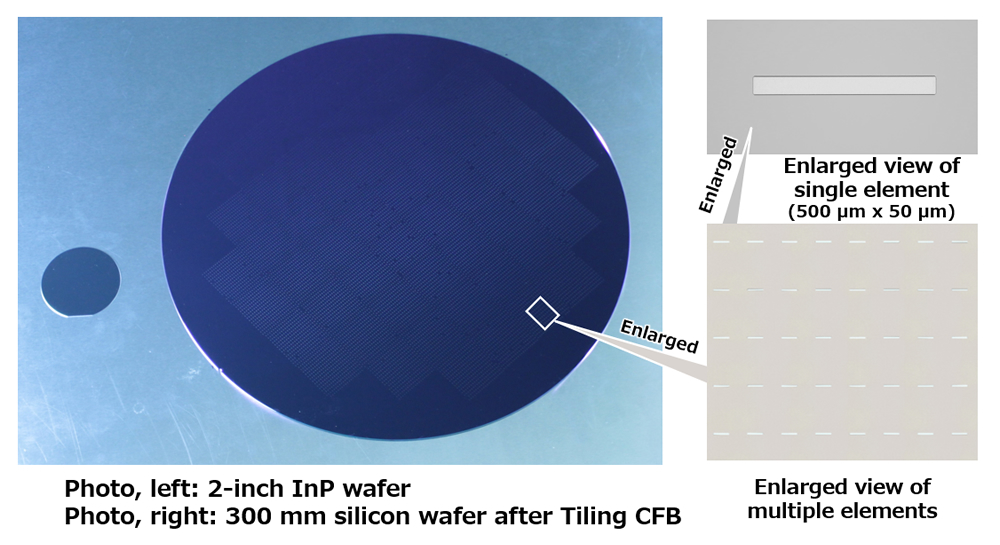
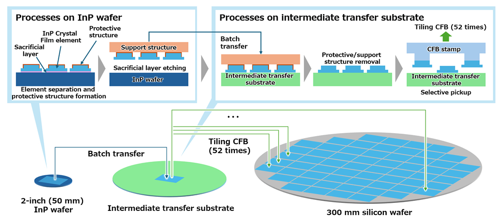
The tiling CFB technology OKI developed overcomes this disparity in wafer sizes and allows heterogeneous integration without causing damage. The technology allows for 52 repeated tiling operations over the entire surface of a 300mm silicon wafer using a single 2-inch InP wafer, enabling efficient use of InP-based materials. The InP wafer can be reused as is after transfer to allow material recycling and reuse, helping reduce the environmental burden. Placement accuracy is approximately ±1 µm, with an angular accuracy of ±0.005°. This high accuracy, when combined with OKI’s proprietary 3D intersecting waveguide silicon photonics technology, realizes high-efficiency optical coupling between optical semiconductors and silicon waveguides.
Novel Process Technology
Furthermore, by repeatedly transferring Crystal Films from the intermediate transfer substrate using a CFB stamp, OKI has established Tiling CFB technology that enables tiling over the entire surface of a 300mm silicon wafer. The CFB stamp has a structure capable of selectively transferring only the Crystal Films required, and repeated transfer enables efficient tiling. The capacity to repeatedly transfer lower-density arrays of Crystal Films required for the device from a high-density array of Crystal Films arranged on the intermediate transfer substrate allows effective use of materials without waste. Measuring 30 mm × 30 mm, the CFB stamp used in this demonstration completed 52 transfers onto the entire surface of a 300 mm silicon wafer in approximately 10 minutes, sufficient for commercial production.
This demonstration proved the feasibility of Tiling CFB technology in the transfer from 2-inch wafers to 300mm silicon wafers. The technology can also be adapted as necessary to allow use with 3- or 4-inch InP wafers and 200mm silicon wafers. Since it can also be applied with existing optical semiconductor products, it will help improve performance by permitting transfer to high heat-dissipation substrates and productivity by allowing use of larger wafer sizes.
- Share: