ASIA ELECTRONICS INDUSTRYYOUR WINDOW TO SMART MANUFACTURING
OKI to Surge More Capacity With Improved PCB Line
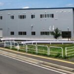
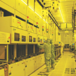
The OKI Group PCB business company OKI Circuit Technology has set up a new ultra-high-multilayer PCB line at the Joetsu Plant in Joetsu City, in Japan’s Niigata Prefecture. Accordingly, it already started its full-scale operations in July.
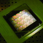
The PCBs produced in the said line will go into equipment for manufacturing and testing semiconductors for applications involving AI, data centers, and next-generation communication networks. Moreover, the new line enables high-precision and high-definition circuit formation which supports a via pitch (Note 1) of 0.23 mm. At the same time, it has increased production capacity by approximately 1.4 times compared to previous levels. Thus, the company is strengthening the capability for manufacturing of a wide variety of products in small quantities.
In addition, OKI also aims to expand sales by targeting manufacturers of semiconductor manufacturing and testing equipment.

Evolving Semiconductor Trends
Semiconductors have been evolving dramatically, with increased functionality, reduced size, lower power consumption, and greater capacity. Along with miniaturization and multilayering, progress has also been made in the development of technologies and new materials. This aims to achieve high-voltage resistance. At the same time, large-capacity data processing, and high-speed transmission.
Thus, his has led to higher numbers of terminal pins and reduced pitches to handle large-volume data processing. The PCBs used for manufacturing and function testing of these next-generation semiconductors are necessary to have narrow pitch and ultra-high multilayering of more than 100 layers. This requires the development of new ultra-thin materials to ensure low thickness, even when multilayered, and manufacturing technologies such as ultra-fine hole drilling. That is, capable of accurately penetrating microscopic circuits on multilayer boards.
Expands Area by 1.2 Times
Because of these developments, OKI has decided to expand the manufacturing area within the Joetsu Plant by 3,300sq.m. This is about 1.2 times the previous area. Most importantly, the line now includes a new surface treatment line for handling ultra-thin materials and additional direct imaging equipment. The AOI (Note 2) automated inspection equipment has also been relocated. Therefore, this will optimize the flow of the PCB production process, improve production quality and increase production capacity by about 1.4 times.
The new line has also achieved improved line width accuracy (stabilization of transmission characteristics) using high-precision circuit formation and a high-definition etching line. This has been possible by reinforcing automatic transport and direct imaging equipment for materials. Specifically, ranging from ultra-thin 0.03 mm to thick 8 mm boards.
OKI Circuit Technology President Masaya Suzuki said the installation of additional high-precision drilling equipment has improved OKI Circuit Technology’s capabilities. Particularly, in ultra-fine hole drilling with diameters of 0.10 mm or less. Thus, enabling ultra-high multilayer and high-definition PCBs with over 110 layers. This will meet customer demands for next-generation semiconductor manufacturing and testing.
OKI is currently focusing on its EMS business, which provides one-stop comprehensive Mono-zukuri services from design to manufacturing and reliability testing. The installation of this new line forms part of its technological development and production ramp-up investment in fields promising future growth within the PCB business, such as semiconductors, aerospace, defense, robotics, and next-generation communications. OKI aims to maintain active development of PCBs and manufacturing technologies in response to advancements in related technologies.
Notes:
[Terminology]
Note 1: Via pitch
Distance between holes (via holes) that electrically connect conductors; the smaller the distance, the greater the manufacturing challenges.
Note 2: AOI (Automated Optical Inspection)
Automated visual inspection in the manufacturing of PCBs and LCD panels, which uses cameras to autonomously scan target components to identify missing parts, fillet (rounded corner) size and shape, and distortion.
20 August 2024
- Share: