ASIA ELECTRONICS INDUSTRYYOUR WINDOW TO SMART MANUFACTURING
Applied Materials, GF to Grow Photonics Role in AI
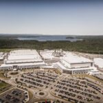
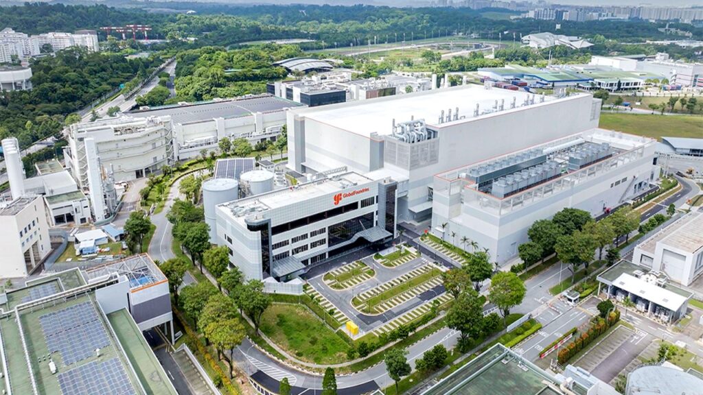
Applied Materials, Inc. and GlobalFoundries (GF) have sealed a strategic collaboration that will propel the role of photonics in artificial intelligence (AI) applications. Specifically, both companies agreed to establish a state-of-the-art waveguide fabrication facility at GF’s Singapore site to accelerate the emerging photonics inflection driven by AI.
The collaboration marks a significant milestone in the evolution of photonics as a foundational technology for next-generation AI applications, including augmented reality (AR) and human-centric digital experiences that require ultra-efficient, lightweight and high-performance optical systems.
Delivers Innovative Tech Solutions
Applied Materials will develop waveguide components with GF as its high-volume manufacturing partner in Singapore, leveraging decades of semiconductor expertise. The alliance leverages on Applied Materials’ materials engineering expertise while GF for its semiconductor manufacturing capabilities.
Dr. Paul Meissner, Vice President and General Manager of Applied Materials’ Photonics Platforms Business in the Office of the CTO said photonics is rapidly becoming a critical enabler of augmented reality glasses, with humans at the center of the AI experience. Therefore, Applied Materials is in a unique position to lead the transformation.
“The collaboration with GlobalFoundries allows Applied to extend our leadership in materials engineering and deliver highly integrated display technologies,” said Meissner.
Meanwhile, Yew Kong Tan, senior vice president and general manager, APAC Manufacturing and Singapore Site at GF. “By combining our global semiconductor manufacturing expertise with Applied’s cutting-edge materials engineering, we’re delivering innovative technology solutions that will drive and scale adoption of next generation devices.”
The collaboration builds on the emerging and vibrant photonics ecosystem in Singapore, encompassing materials, sensors, integration, assembly, test, and applications.
24 September 2025
- Share: