ASIA ELECTRONICS INDUSTRYYOUR WINDOW TO SMART MANUFACTURING
Imec’s Breakthrough 300mm GaN uses Shin-Etsu Substrate
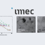
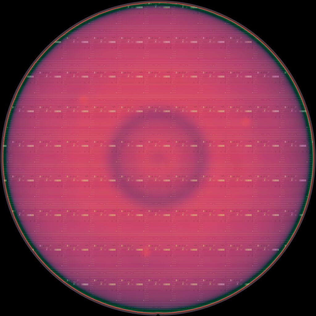
The QSTTM substrate*1, a 300mm GaN growth substrate that Shin-Etsu Chemical Co., Ltd. developed, has been adopted for the 300mm GaN power device development program at IMEC*2, where sample evaluation is in progress. In the evaluation, the 5µm-thick HEMT*3 device using a QSTTM substrate achieved a record-breaking voltage resistance exceeding 650 V for a 300mm substrate.
Achieves World Record
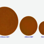
Shin-Etsu Chemical, licensed by QROMIS, Inc., manufactures 150mm and 200mm QST™ substrates, as well as GaN-on-QST™ epitaxial substrates of various diameters. In September 2024, the company started providing 300mm QST™ samples in a joint initiative with QROMIS.
Furthermore, Shin-Etsu Chemical and QROMIS have established a close partnership to provide 300mm QST™ substrates for the state-of-the-art 300mm CMOS fab of imec, which is based in Leuven, Belgium. IMEC is a 300mm GaN power device development program*4 that was officially launched in October 2025, announcing its plan to develop a GaN power device using 300-mm QSTTM.
imec developed a 650V-rated product, to be followed by a 1200 V+ withstand voltage model, targeting AI data center, industrial, and automobile applications.
The initial evaluation results showed that imec has successfully fabricated a 5µm-thick high-voltage GaN HEMT structure on Shin-Etsu Chemical’s 300-mm QST™ substrate in compliance with the SEMI standards, using Aixtron*5‘s Hyperion MOCVD equipment.
This achieved a world record breakdown voltage of over 800V, significantly exceeding 650V on substrates compliant with SEMI standards, demonstrating excellent in-plane uniformity. These results demonstrate that the QST™ substrate, whose thermal expansion coefficient is matched to GaN, can stably deliver excellent GaN crystal growth performance even at large diameters.
Reduces Production Costs
Because Shin-Etsu Chemical’s existing silicon wafer production line can be used for GaN, increasing the substrate diameter is expected to reduce production costs. However, GaN growth on silicon wafers suffers from increasingly poor production yields at larger diameters due to issues such as wafer warpage, preventing practical mass production.
The 300mm QST™ substrate solves this issue by enabling the epitaxial growth of thick-film 300mm GaN for high-voltage applications without warping or cracks—previously unattainable on silicon wafer substrates. Thus, significantly reducing device costs.
To date, Shin-Etsu Chemical has been enhancing facilities for 150mm and 200mm QSTTM substrates and is currently working toward the mass production of 300mm QSTTM substrates.
The QSTTM substrates are currently being evaluated by many Japanese and international customers for applications such as power devices, high-frequency devices, and LED devices. They are currently in the development phase for practical applications to address the recently increasing interest in AI data center power supplies.
The lineup of the 150 to 300mm QSTTM substrates can help significantly accelerate the spread of various GaN devices. Shin-Etsu Chemical is committed to furthering the social implementation of GaN devices, combining essential characteristics for our future society, to contribute to the realization of a sustainable society where energy can be used efficiently.
Notes:
*1: The QSTTM substrate is a substrate of composite materials dedicated to GaN growth developed by QROMIS (CA, U.S.A., CEO: Cem Basceri) and was licensed to Shin-Etsu Chemical in 2019. QSTTM is a U.S. trademark of QROMIS (registration No. 5277631).
*2: A world-leading international nonprofit research and development organization in semiconductor technology, headquartered in Leuven, Belgium.
*3: An abbreviation for “High Electron Mobility Transistor.” A field-effect transistor (FET) with a heterostructure where electrons are supplied and transported in separate layers, using compound semiconductors (such as gallium arsenide and gallium nitride). (Offers higher speed and frequency operation than conventional Si transistors due to extremely high electron mobility.)
*5: A multinational company headquartered in Herzogenaurach, Germany, that develops and sells compound semiconductor manufacturing equipment, mainly GaN MOCVD equipment and SiC epitaxial growth equipment.
14 November 2025
- Share: