ASIA ELECTRONICS INDUSTRYYOUR WINDOW TO SMART MANUFACTURING
Breakthrough Brings 2D Transistors to 300mm Wafers
Industry leaders ASML, TSMC, and imec have unveiled a major semiconductor milestone, showcasing a scalable 300mm integration process for 2D-material transistors. Presented at the 2026 IEEE/JSAP Symposium on VLSI Technology and Circuits, the development marks a significant step toward transitioning 2D transistor research from laboratory environments into full-scale manufacturing.
ASML is a Netherlands-based manufacturer of semiconductor lithography machines while TSMC is a Taiwanese chipmaker, both working together with Belgian research hub imec to advance 2D transistor integration.
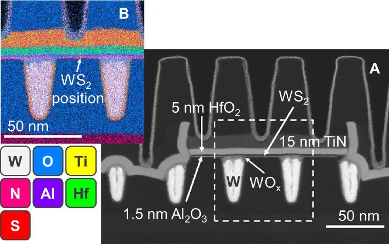
The collaboration demonstrated both n-type and p-type field-effect transistors (FETs) using transition metal dichalcogenides (TMDs), including MoS2, WS2, and WSe2. For the first time, these devices were produced with a 50nm contacted poly pitch (CPP) at an industry-relevant scale, while maintaining strong electrical performance.
Scaling 2D Materials for Advanced Logic
TMD-based transistors have long been viewed as promising alternatives to silicon for future semiconductor nodes. Their atomically thin structure enables improved electrostatic control and supports scaling at extremely small dimensions. These characteristics make them attractive for ultra-scaled logic applications, as well as back-end-of-line (BEOL) and wafer backside integration.
However, industry adoption has faced challenges due to the lack of scalable manufacturing approaches compatible with 300mm wafers. Existing demonstrations have largely remained confined to laboratory settings or larger device geometries. The newly introduced integration flow addresses this barrier by combining scalability with performance retention.
Key Performance Gains and Industry Firsts
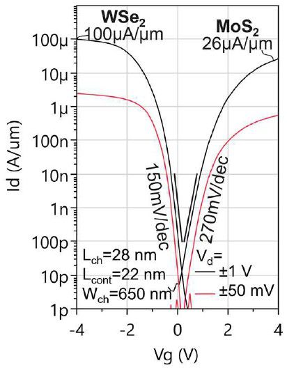
The joint effort achieved several critical milestones. Researchers demonstrated both nFETs and pFETs at a 50nm CPP, marking a first for 2D materials at this scale. The devices also exhibited low off-current at zero gate voltage, indicating efficient switching behavior. Additionally, pFETs based on WSe2 showed performance levels approaching leading lab-based benchmarks.
The integration approach delivers strong manufacturing viability, with 94% of fabricated devices meeting operational criteria. Importantly, both transistor types were integrated on a single 300mm wafer, validating a CMOS-compatible process flow.
Accelerating Lab-to-Fab Transition
A key enabler of this advancement is the use of single-pattern extreme ultraviolet (EUV) lithography. Developed in close collaboration with ASML, the technique provides the resolution needed to achieve aggressive scaling targets, including channel lengths as small as 28nm.
The process also incorporates an innovative fabrication flow. Unlike conventional designs, the transistors use bottom contacts with an overlapping gate structure.
Industry leaders view the development as a critical step in accelerating the commercialization of 2D materials. By delivering a robust and scalable integration path, the collaboration aims to reduce risk in adopting new transistor architectures and shorten the transition timeline from research to production.
The approach is also material-flexible, meaning it can be extended to other 2D channel materials beyond those demonstrated. This opens wider opportunities for innovation in future semiconductor nodes.
Positioning 2D Materials for Future Chips
As semiconductor scaling approaches the limits of silicon, 2D materials are emerging as a viable path forward. The demonstrated 300mm integration proves that these materials can meet both performance and manufacturing requirements at advanced dimensions.
With strong electrical results, high yield, and compatibility with established fabrication processes, the breakthrough positions 2D-material transistors closer to real-world deployment in next-generation chips.
16 June 2026
- Share: