ASIA ELECTRONICS INDUSTRYYOUR WINDOW TO SMART MANUFACTURING
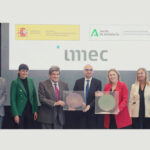
Infinitesima to Join imec-ASML Innovative Chip R&D
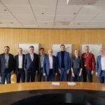
Infinitesima will be joining a project with research institute imec and ASML Holding that aims to develop solutions to advance the semiconductor industry. The Britain-headquartered Infinitesima, a known provider of advanced metrology solutions for the semiconductor industry, will be joining the project for a period of three years.
Advancing Inspection, Metrology
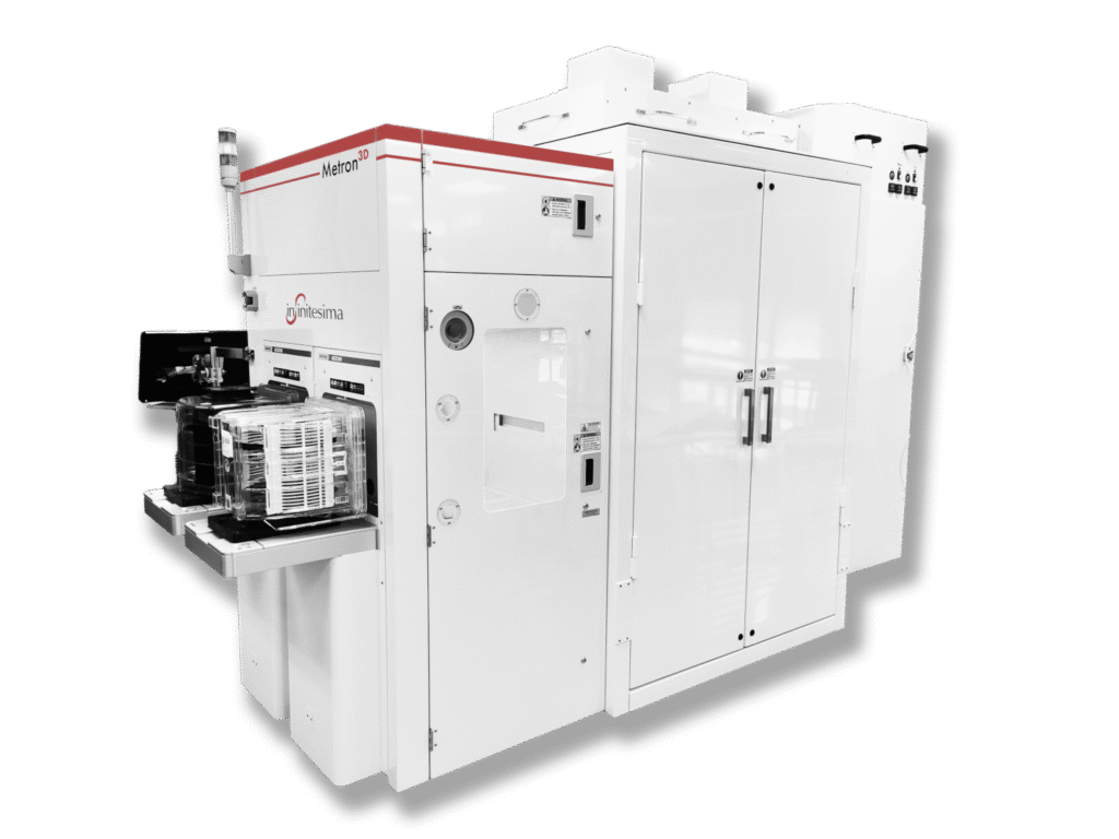
As part of this project, Infinitesima will be siting its Metron3D 300 mm in-line wafer metrology system at imec. The system will be used to advance next-generation device development by partners including ASML to continue with the characterization and development of high- NA EUV resist imaging. Infinitesima will work closely with imec to develop new tool capabilities and enhancements. This joint effort aims to deliver true 3D process control – critical for enabling the production of future semiconductor devices.
Infinitesima’s partnership with imec began in 2021, starting with enabling tip-induced nanoscale tomographic sensing using its patented Rapid Probe Microscope (RPM)™ for research and failure analysis applications. This new collaboration marks the expansion of the Infinitesima-imec partnership into high-speed, in-line production metrology, supporting the semiconductor industry’s advancing inspection and metrology demands for sub-nanometer features and increasingly complex 3D structures.
The Metron3D 300 mm in-line wafer metrology system will be used to optimize and explore metrology solutions for cutting-edge applications, including hybrid bonding, high-NA EUV lithography and 3D logic device structures such as complementary field-effect transistors (CFETs). This project will combine the extensive expertise of the project partners with Infinitesima’s RPM technology, enabling in-depth three-dimensional (3D) surface detection, high-speed imaging, and interferometric accuracy.
With this expanded partnership, Infinitesima is set to reinforce its leading position in in-line semiconductor metrology, supporting the industry’s evolution toward smaller and increasingly complex device architectures.
“We are delighted to extend our existing collaboration with imec to support the critical metrology challenges of some of the most critical process steps for next generation semiconductor processes,” said Peter Jenkins, CEO of Infinitesima.
Chip Research in Europe
ASML and imec forged last March a five-year strategic partnership focusing on research and sustainability that will advance the semiconductor industry.
The collaboration incorporates ASML’s whole product portfolio, with a focus on developing high-end nodes, using ASML systems including 0.55 NA EUV, 0.33 NA EUV, DUV immersion, YieldStar optical metrology, and HMI (Hermes Microvision) single- and multi-beam technologies. These tools will be installed in imec’s state-of-the-art pilot line and incorporated in the NanoIC pilot line, which is funded by the European Union (EU) and the Flemish government. Particularly, the line provides the most advanced infrastructure for sub-2nm R&D to the international semiconductor ecosystem.
25 July 2025
- Share: