

ASIA ELECTRONICS INDUSTRYYOUR WINDOW TO SMART MANUFACTURING
ASML Unites With Chip Giants to Advance High-NA EUV
ASML has strengthened its position at the center of the semiconductor industry’s next technology transition through separate strategic collaborations with Intel Foundry, Samsung Electronics and TSMC. While each partnership has a distinct focus, together they signal growing industry alignment around High Numerical Aperture Extreme Ultraviolet (High-NA EUV) lithography as a key enabler of future semiconductor innovation.
The announcements, unveiled around the SPIE Photomask Technology and Extreme Ultraviolet Lithography events, span three critical areas: production deployment, memory manufacturing and ecosystem preparation for larger-format photomasks. Collectively, they reflect a coordinated industry effort to support rising demand for advanced chips in the AI era.
Intel and ASML Highlight Manufacturing Readiness
Intel Foundry and ASML emphasized the growing maturity of High-NA EUV technology. According to the companies, Intel has processed more than one million wafers through a combination of tool certification, research and development, testing and volume production activities. High-NA EUV is already being used on select layers of certain Intel Core Ultra Series 3 processors, code-named Panther Lake, with overlay, throughput and availability meeting expectations.
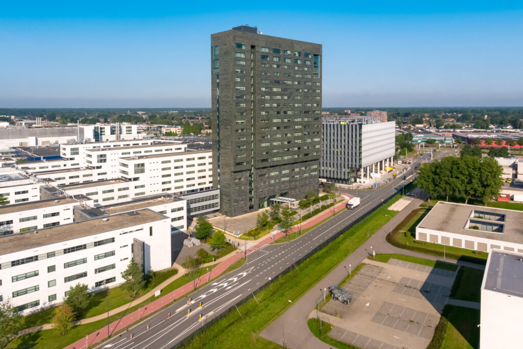
The partners also stressed that customers can benefit from High-NA EUV using today’s 6-inch mask format, supported by design optimization and stitching capabilities, while the industry prepares for larger mask formats in the future.
“Intel Foundry has been one of the key leaders of the industry’s adoption of High NA,” said Christophe Fouquet, President and CEO of ASML. “ASML recognizes Intel Foundry’s pioneering role in High NA and its innovations to deliver value today with 6-inch masks.”
Naga Chandrasekaran, Executive Vice President and Co-General Manager of Intel Foundry, said the semiconductor industry requires manufacturing innovations that are both production-ready and easy to implement for increasingly complex AI products.
Samsung Expands High-NA EUV Into Advanced Memory
Meanwhile, Samsung Electronics and ASML announced an expansion of their long-standing strategic partnership focused on next-generation semiconductor manufacturing.
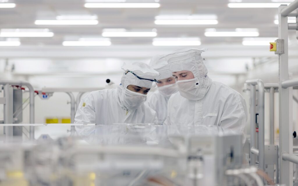
A major element of the collaboration is Samsung’s decision to participate in the industry’s 12-inch photomask initiative. In addition, Samsung plans to introduce High-NA EUV into future DRAM high-volume manufacturing by 2028. The move would mark the first planned use of the technology in volume DRAM production and is expected to support continued memory scaling through improved resolution and greater manufacturing efficiency.
“The AI era is transforming the semiconductor industry and increasing the importance of technological innovation across the entire value chain,” said Young Hyun Jun, Vice Chairman and CEO of Samsung Electronics.
Fouquet added, “As the industry enters a new era driven by artificial intelligence, close collaboration with our customers becomes even more important.”
TSMC and ASML Lead Photomask Transition
At the same time, TSMC and ASML launched a collaborative initiative to help guide the semiconductor industry’s transition to 12-inch photomasks for High-NA EUV lithography.
The initiative aims to establish a 12-inch mask pilot line by 2031 and support full lithography system readiness for advanced-node production by 2033.
The companies said larger masks are expected to increase productivity, reduce chipmaking costs and eliminate stitching constraints, enabling manufacturers to maximize High-NA EUV capabilities.
“We expect the adoption of High NA EUV to increase progressively along the device scaling roadmap,” said Fouquet.
TSMC Chairman and CEO Dr. C.C. Wei added: “When the industry works together to solve complex problems, we unlock possibilities that no single company could achieve alone.”
Ecosystem Momentum Builds Around High-NA EUV
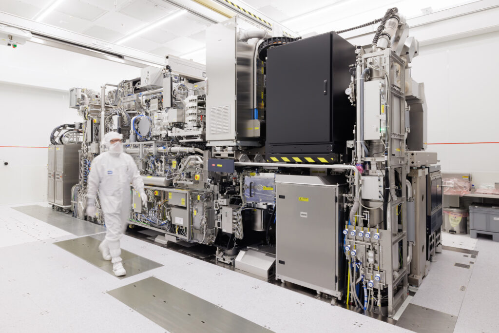
Although the three announcements address different challenges, they collectively reveal a broader industry strategy. Intel is demonstrating production readiness, Samsung is extending High-NA EUV into advanced memory manufacturing, and TSMC is helping build the infrastructure needed for future scaling.
Together with ASML, the companies are advancing the technologies, standards and ecosystem collaboration required to support the next generation of AI-driven semiconductor innovation.
08 September 2026
- Share: