



ASIA ELECTRONICS INDUSTRYYOUR WINDOW TO SMART MANUFACTURING
Redefining Advanced Packaging Yield: OMRON Harnesses 3D CT X-ray, Digital Twins
Driven by surging demand for AI computing, advanced packaging technologies such as glass substrates with through-glass via (TGVs), Micro Bumps, and Chiplets are advancing rapidly. Non-destructive inspection has transformed from a mere quality control check into a vital cornerstone of process optimization.
At SEMICON Taiwan 2026, OMRON brought together three of its major business divisions under its core technology, Sensing & Control + Think, to present 3D-CT X-ray inspection system, NVIDIA Omniverse-powered digital twins, and advanced wafer and panel handling solutions from its Semiconductor Incubation Center (SIC). To address frontline manufacturing challenges, OMRON screened an interview video featuring Dr. Jen-Jun Chen, Senior Director of Corporate R&D / MPDD at ASE Inc. should be used from semiconductor R&D through mass production in the AI era.

Bridging R&D and Mass Production: Building a Unified Quality Data Pipeline
A central challenge in advanced packaging development is the discrepancy in inspection standards between analysis during R&D, which requires maximum resolution, and mass production, which prioritizes high throughput. OMRON resolves this by establishing a unified “Quality Data” pipeline spanning R&D to high-volume manufacturing. During the R&D stage, detailed 3D-CT data is collected to establish precise process windows. As products transition to mass production, inspection focuses on high-risk defect areas to maximize yield and line throughput.
In the interview, ASE’s Dr. JJ Chen suggested that quality data in advanced packaging is no longer just a binary Pass/Fail result, but an essential basis for strategic engineering decisions. Guided by the principle that “what cannot be measured cannot be managed,” access to reliable 3D geometry and defect data allows R&D teams to build upon verified baselines rather than starting from scratch, significantly accelerating process development and time-to-market.
Overcoming Next-Gen Packaging Challenges: Glass Substrates, Warpage, and Internal Defects
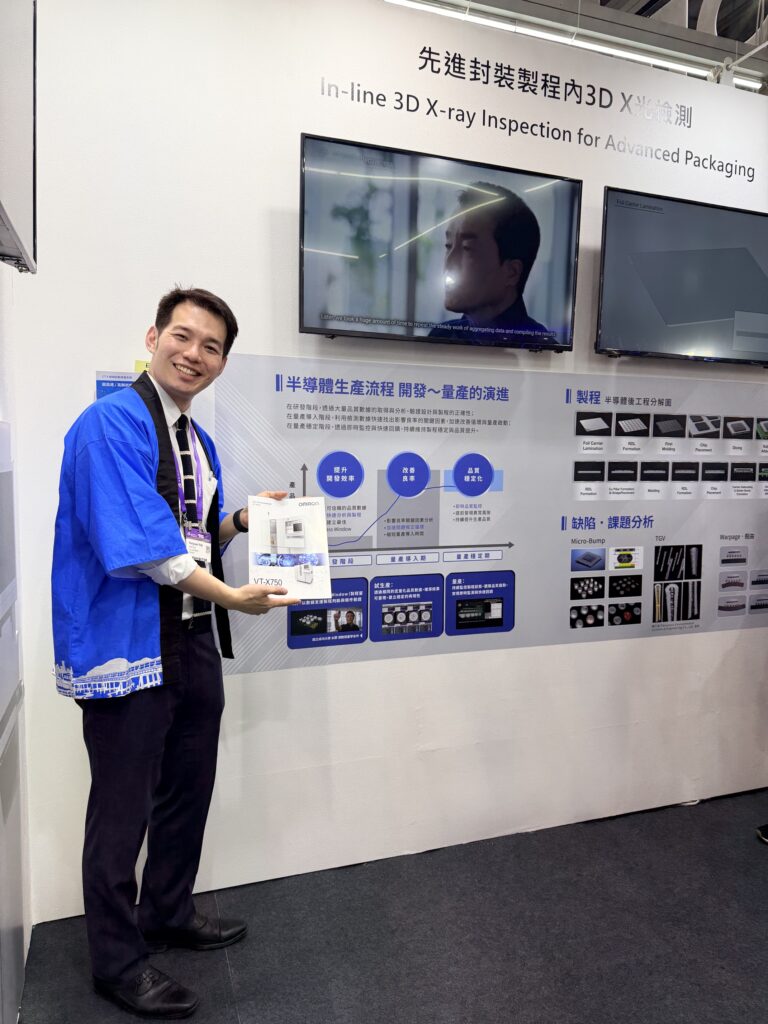
In panel-level packaging and glass substrate processes, differences in the coefficients of thermal expansion between dissimilar materials can lead to warpage, cold joints, and internal micro-voids. Automated optical inspection (AOI) inspects only surface features, while 2D X-ray lacks the depth resolution needed to characterize complex 3D internal structures.
OMRON’s 3D-CT X-ray non-destructive inspection system images multilayer internal structures without damaging increasingly sophisticated semiconductor chips, visualizing and quantifying bonding defects, micro-voids, and other internal features. This enables the detection of potential defects that may not be revealed by functional testing but could lead to failures as physical changes occur during product use.
In addition to inspection system, OMRON showcased panel handling, sensing, and safety control solutions. By integrating these handling mechanisms with vision and 3D-CT X-ray inspection systems, OMRON supports more efficient and stable semiconductor manufacturing processes.
Digital Twin Applications: NVIDIA Omniverse and AI Reasoning
Through its collaboration involving NVIDIA Omniverse, powered by OpenUSD, OMRON supports the development of a data platform that adds semantic information to extensive inspection data collected under varying conditions, enabling AI-driven use and search. Integrating manufacturing parameters into a digital twin environment allows engineers to interact with AI models conversationally in their native language using natural language reasoning. Furthermore, incorporating Video Search & Summarization (VSS) technology to analyze equipment behavior and image data enables manufacturing teams to move from reactive defect detection toward root cause identification and process optimization.
Global Infrastructure Supporting Cross-Border Semiconductor Expansion
As Taiwanese foundries and OSAT leaders actively establish manufacturing hubs across Japan, the United States, and Southeast Asia, OMRON supports these global strategies through an established international network.
08 September 2026
- Share: