


ASIA ELECTRONICS INDUSTRYYOUR WINDOW TO SMART MANUFACTURING
Kyocera, Tohoku Advance AI Data Center Optics
Kyocera Corporation and Tohoku University have announced the development of what they describe as the world’s first technology to directly integrate optical isolators onto silicon photonics chips using a laser annealing process. The innovation is designed to address critical performance challenges in next-generation optical communication systems and AI-driven data centers.
According to the organizations, the new isolator-integrated photonics chip reduces back-reflected light by approximately 95%, helping improve optical signal stability while supporting faster and more energy-efficient data transmission.
The research findings were published on September 2, 2026, in the IEEE Access journal.
Growing AI Demand Drives Need for Advanced Photonics
As generative AI applications continue to increase data traffic worldwide, the industry is seeking technologies capable of delivering greater speed and lower power consumption. Silicon photonics has emerged as a promising solution because it enables the transmission and processing of information using optical signals on semiconductor substrates.
At the same time, demand is rising for Co-Packaged Optics (CPO), which combines optical and electronic circuits within a single semiconductor package. This architecture shortens signal paths and reduces both signal loss and energy consumption.
However, reflected light remains a significant challenge in optical circuits because it can interfere with laser performance. Optical isolators solve this problem by allowing light to travel in only one direction.
Laser Annealing Enables Direct Chip Integration
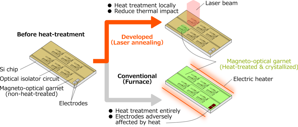
Traditional optical isolators rely on magneto-optical garnet, a crystalline material that requires heat treatment at temperatures exceeding 600°C. Conventional processing heats an entire chip, creating the risk of damage to electrodes, wiring and other integrated components.
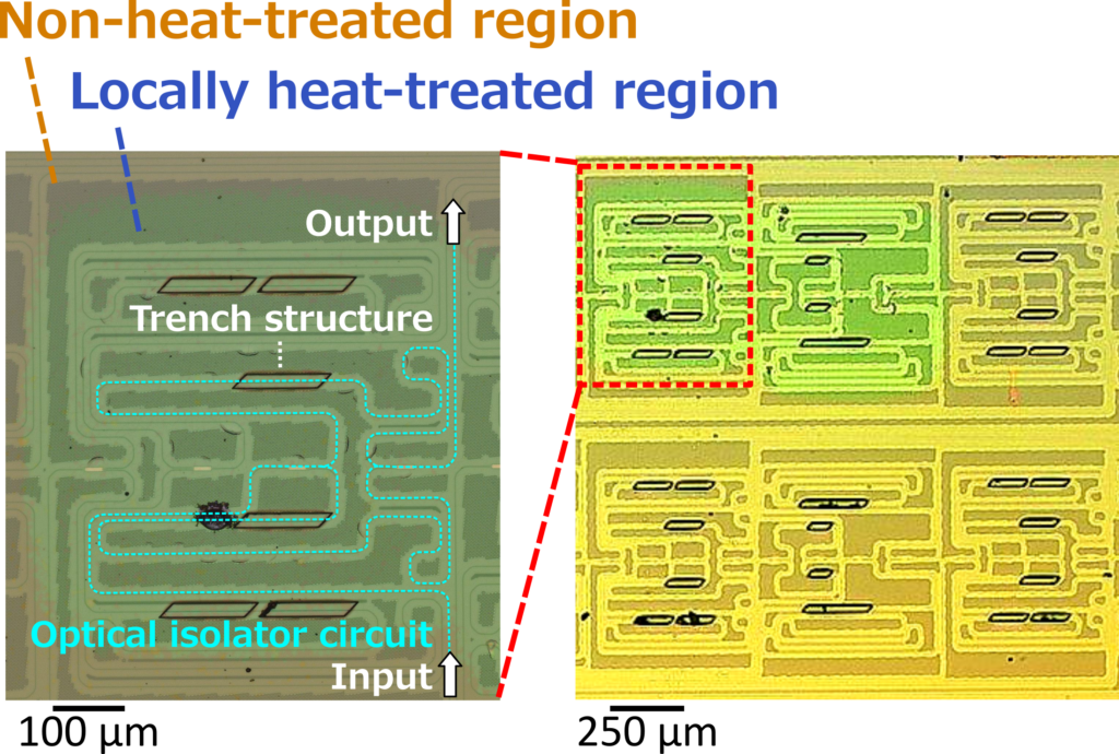
To overcome this limitation, Kyocera and Tohoku University developed a monolithic integration technology that uses localized laser annealing. The technique applies a near-infrared laser only to the specific section of the chip containing the magneto-optical garnet film.
As a result, the garnet material can be crystallized without exposing surrounding optical circuits and electronic components to excessive heat.
Kyocera and Tohoku University stated that they developed “a new technology for integrating optical isolators onto silicon photonics chips using ‘laser annealing,’ a localized, laser-based heat-treatment method.”
Successful Demonstration Validates Performance
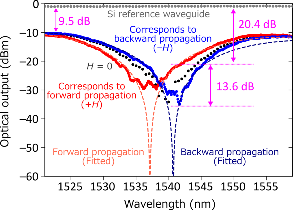
Using the new process, the research team fabricated and tested an optical isolator structure based on light interference.
Experimental results demonstrated an isolation ratio of 13.6 dB within optical communication wavelengths. The tests also confirmed that back-reflected light was reduced by approximately 95%.
Furthermore, electron microscopy verified successful crystallization of the magneto-optical garnet on the silicon waveguide in the laser-treated area.
Commercialization Efforts Continue
The two organizations said they will continue joint development efforts to improve efficiency, reduce losses and enhance manufacturing productivity for large-scale production.
The partners believe the technology could contribute significantly to future optical communication platforms and help support the development of a more efficient and sustainable information society.
12 September 2026
- Share: