ASIA ELECTRONICS INDUSTRYYOUR WINDOW TO SMART MANUFACTURING
OKI Develops New Ultra-Small Optical IC Chip
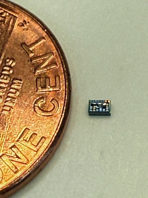
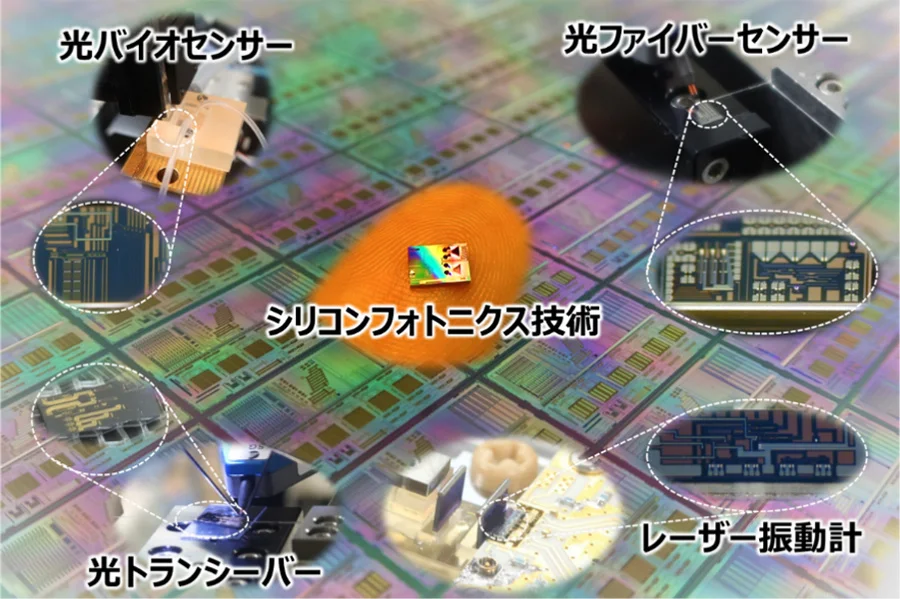
OKI Electric Industry Co., Ltd. has developed an ultra-compact optical integrated circuit chip that can be applied to a variety of applications, such as optical fiber sensors, laser vibrometers, and optical biosensors, using silicon photonics technology, which is a semiconductor for optical circuits. With the new optical chip, it is possible to achieve ultra-miniaturization and low power consumption similar to LSI (Note 1). Also, it enables overwhelming cost reduction through mass production of optical sensor modules.
Mainly, optical sensors are technologies that detect, process, and transmit physical phenomena such as vibration, distortion, and temperature as light using optical fibers and optical waveguides with low optical loss. They are themselves green technologies that realize sensing with low energy savings.

Meanwhile, silicon photonics technology is a technology that can expand the application area of optical sensors, which was previously limited to local use. It can be expected to make a significant contribution to the progress of green transformation (GX)(Note 2).
In response to various issues facing modern society, such as aging social infrastructure, labor shortages, environmental problems, and the extension of healthy life expectancy, high-precision sensor technology and network technology that smoothly collects vast amounts of sensor data are required. Mainly, high-precision optical sensors that utilize the properties of light with low energy loss are one of the effective technologies to achieve this. However, because they are large and expensive, they have only been applied to a part of the technology, such as research applications and large-scale infrastructure.
Historically, OKI has been engaged in the research and development of silicon photonics technology, focusing on transceivers for optical communications. The company continues to develop various optical sensors by adding them to the company’s research targets.
Silicon Photonics Technologies
Silicon photonics technology is a technology that integrates complex optical circuits. They are realized by wiring individual optical components with optical fibers into integrated circuits on a silicon substrate using semiconductor microfabrication technology. Since it uses the same manufacturing method as LSI, which is indispensable for computers, it is possible to reduce size and weight, save energy, and reduce costs through mass production. Devices that were previously large, heavy, and difficult to handle can be realized in the same size as a smartphone or tablet, dramatically expanding the application area of optical sensors.
In November 2023, OKI announced its technology strategy until 2031 to realize an “edge platform.” Specifically, the “Edge Platform” is a technological concept that expands the value provided by upgrading the edge and connecting data based on OKI’s core competence of “toughness,” which has supported social infrastructure. In the company’s technology strategy, it is strengthening optical sensing technologies in a wide range of fields, from social infrastructure monitoring to the medical field. Mainly, the development of this photonic integrated circuit chip is the result of making full use of silicon photonics technology based on this technology strategy.
Generally, OKI will continue to expand into more diverse fields by promoting large-scale photonics integrated circuits, including semiconductor materials such as light sources that are different from silicon, and photonics-electronics convergence, based on silicon photonics technology. Ultimately, we aim to realize a universal integrated circuit chip that can programmatically implement various functions on a single chip, and will utilize it as the core of green technology.
This content will be exhibited at “OKI WORLD 2024” to be held in October 2024, and the actual operation of laser vibrometer and optical biosensor is scheduled to be demonstrated. You can see a wide variety of optical integrated circuit chip designs, including fiber optic sensors, laser vibrometers, optical sensor chips for optical biosensors, and optical transceiver chips for next-generation optical access networks.

Application Samples
The new optical circuit can be applied to the following applications.
Fiber optic sensor
Miniaturization and low cost reduction by optical integration can be expanded to the monitoring and maintenance of all kinds of social infrastructure such as bridges, tunnels, and slopes.
Laser vibrometer
It can be miniaturized to about 1/200,000 of the volume ratio of conventional optical circuits, can be mounted on drones and robots, and contributes to the sophistication and labor saving of equipment inspections by taking advantage of a wider frequency response than general vibration meters.
Optical biosensor
Enables quick and easy identification of a variety of different biosubstances, contributing to the advancement of testing in the fields of biotechnology and healthcare.
Optical transceiver
Ultra-compact, low-cost, high-speed transceivers for optical access networks can be realized, contributing to large-capacity data communication
Terminology
Note 1: LSI (Large-Scale Integration)
A device in which microscopic electronic components and wiring are densely integrated on a semiconductor chip such as silicon
Note 2: GX(Green Transformation)
Initiatives to Reduce Greenhouse Gas Emissions and Realize a Sustainable Society
This is an online translation of a Japanese press release with slight editing made by Dempa.
-09 October 2024-


