



ASIA ELECTRONICS INDUSTRYYOUR WINDOW TO SMART MANUFACTURING
Industry Leaders Unite to Speed Chip Packaging
The Global Electronics Association and the Fraunhofer Group for Microelectronics have signed a Memorandum of Understanding (MoU) aimed at accelerating the industrial adoption of advanced packaging technologies. The collaboration seeks to bridge one of the semiconductor industry’s most persistent challenges: transforming promising pilot-line innovations into scalable, manufacturable solutions.
At the center of the initiative is APECS, the European pilot line for Advanced Packaging and Heterogeneous Integration for Electronic Components and Systems established under the EU Chips Act. Coordinated by Fraunhofer-Gesellschaft and implemented by Research Fab Microelectronics Germany (FMD), APECS provides a platform for developing next-generation packaging technologies designed to support increasingly complex electronic systems.
Linking Technology Innovation with Manufacturing Readiness
As semiconductor devices become smaller, faster and more powerful, advanced packaging has moved from a supporting technology to a strategic enabler of performance and system integration. However, industry experts recognize that technical breakthroughs alone do not guarantee commercial success.
The newly announced partnership addresses that challenge by combining APECS’ innovation infrastructure with the Global Electronics Association’s expertise in standards development, industry engagement, training and knowledge transfer. The goal is to create the frameworks necessary for reliable deployment across global supply chains.
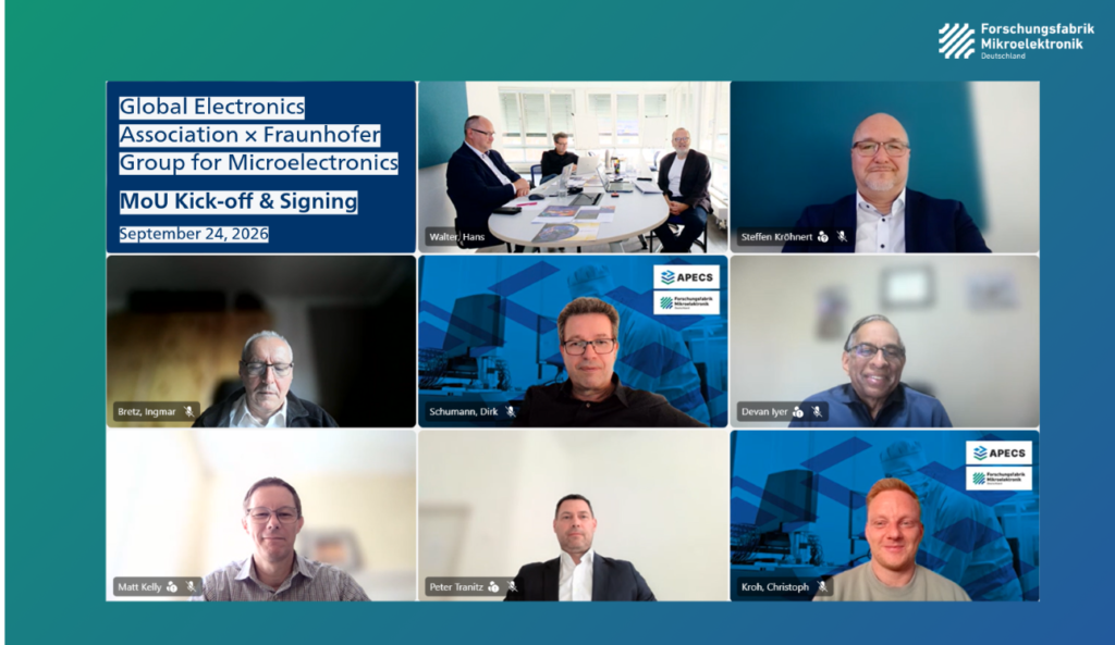
“The strategy of pairing pilot line capability development with industry-wide standardization and enablement will help supply chain readiness ahead of product qualification and manufacturing,” said Devan Iyer, Chief Strategist for Advanced Electronic Packaging at the Global Electronics Association.
Building the Foundation for Advanced Packaging Adoption
APECS provides access to critical capabilities in advanced packaging and heterogeneous integration, including chiplet-based modules and 2.5D and 3D integration technologies. The pilot line also promotes System-Technology Co-Optimization (STCO), an engineering approach that aligns product design, materials selection and manufacturing processes earlier in the development cycle.
Industry leaders increasingly view these capabilities as essential for overcoming performance limitations while enabling more efficient and resilient electronic systems. Yet widespread adoption requires common approaches to design, testing, reliability, manufacturing and data exchange.
“Collaborations like this are about building the practical scaffolding, guidelines, standards, tools and training, that helps suppliers qualify, customers specify, factories operate and regulators trust,” said Matt Kelly, Chief Technology Officer of the Global Electronics Association.
Strengthening Supply Chain Resilience and Interoperability
Beyond technology development, the MoU supports broader industry priorities. These include improving interoperability, enhancing compliance frameworks and strengthening supply chain resilience across the electronics ecosystem.
According to Dr. Dirk Schumann, Director of the APECS pilot line, successful industrial deployment depends on integrating manufacturing requirements early in the innovation process.
“APECS connects design, advanced packaging, assembly, testing and reliability across a European pilot line infrastructure. For these capabilities to translate into industrial use, technical development also needs to reflect standards, manufacturing practices and common interfaces early in development,” Schumann said.
A Strategic Signal for the Global Electronics Industry
The agreement reflects growing recognition that advanced packaging is becoming a defining factor in future semiconductor competitiveness. By aligning pilot-line innovation with industry standards and operational requirements, the partners aim to convert validated technologies into scalable solutions that can be adopted across global manufacturing networks.
For the broader electronics sector, the collaboration represents a significant step toward reducing commercialization barriers while accelerating the transition from research breakthroughs to industrial-scale production. As advanced packaging becomes increasingly central to semiconductor innovation, initiatives that connect technology development with manufacturing readiness are likely to play a crucial role in shaping the industry’s next phase of growth.
30 September 2026
- Share: