ASIA ELECTRONICS INDUSTRYYOUR WINDOW TO SMART MANUFACTURING
Soitec, PSMC Seal New Deal on Innovative Chip Tech
To support demands for a more powerful but energy-efficient chips, Soitec and Powerchip Semiconductor Manufacturing Corporation (PSMC) have announced a strategic collaboration on ultra-thin transistor layer transfer (TLT) technology. Specifically, this technology will support nanometer-scale 3D stacking of semiconductors.
Soitec is a French manufacturer of innovative semiconductor materials while the Taiwan-headquartered PSMC is the world’s seventh-largest pure-play foundry with four 12-inch and two 8-inch fabs in Taiwan.
Soitec has been developing cutting-edge products delivering both technological performance and energy efficiency. Meanwhile, PSMC’s wafer fabs are capable of producing over 2.1 million 12-inch equivalent wafers annually.
First TLT Technology
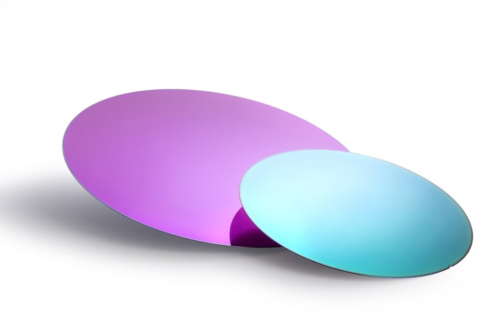
Under the collaboration, Soitec will supply PSMC 300mm substrates incorporating a release layer, Transistor Layer Transfer (TLT) ready. Specifically, this will support a new demonstration of advanced 3D chip stacking at the wafer level. This also marks the first public announcement of Soitec’s TLT technology.
The technology is an enabler for next-generation semiconductor designs that allow for more powerful, compact and energy-efficient chips. Potential applications of these range from smartphones, tablets, and AI devices and even on autonomous driving systems.

Soitec’s Chief Technology Officer and Senior EVP Innovation, Christophe Maleville said the pioneering semiconductor materials unlock new possibilities in chip design and performance. In addition, Maleville said, “Our collaboration with PSMC reflects a shared commitment to pushing the boundaries of 3D integration and supporting the global shift toward more efficient and compact computing architectures. Together we are laying the groundwork for the next generation of semiconductor innovation.”
Meanwhile, PSMC Chief Technology Officer SZ Chang said the company has consistently demonstrated an innovative wafer-stack integrated process by leveraging Soitec’s advanced substrate technology. “The innovation significantly broadens the 3D technology from chip-level stacking – optimizing power performance in computing architecture, to transistor-level stacking – extending Moore’s law, with a remarkable reduction in stacking wafer thickness from micrometer to nanometer level.”
For Faster, Energy Efficient Chips
Soitec’s new TLT technology has enabled them to develop a new substrate stack that allows high-speed transfer of ultra-thin transistor layers into different types of wafers. This technique is a key requirement in heterogenous integration, where diverse chip components are combined in a single package.
Because of this, Soitec is able to meet the industry’s growing demand for faster and more energy-efficient chips. Especially, in this era of artificial intelligence (AI).
The stacking process Soitec has developed enables multiple transistor layers to be built vertically to support 3D transistor architectures, including vertical field-effect transistors (FETs) with backside power delivery networks (PDNs).
This TLT substrate leverages Smart Cut™ technology together with infrared (IR) laser release processing. The proprietary Soitec technology enables the formation of an ultra-thin semiconductor layer, ranging from 5nm to 1µm in thickness, on top of the TLT substrate.
Once devices are fabricated on the TLT wafer, the IR laser process facilitates the lift-off of the ultra-thin layer from the substrate to the target wafer, without introducing thermal stress or damaging the devices.
The Soitec-PSMC collaboration builds on existing France-Taiwan cooperation initiatives in AI and other semiconductor-related domains.
07 June 2025


