ASIA ELECTRONICS INDUSTRYYOUR WINDOW TO SMART MANUFACTURING
Showa Denko Ramps up Capacity of Semiconductor Polishing Materials
Showa Denko Materials Co., Ltd. has decided to expand its production capacity and evaluation functions for CMP slurries*1 polishing materials. These materials are used in the production of semiconductor integrated circuits. Showa Denko Materials will build an additional new plant as part of the investment. Moreover, it will introduce additional production and evaluation equipment at Yamazaki Works and its Katsuta manufacturing site, and its consolidated subsidiary Showa Denko Semiconductor Materials (Taiwan) Co., Ltd. (SDSMT) in Taiwan.
An investment of approximately 20 billion yen (US$139.6 million) is made to meet the growing demand for CMP slurry. Also, it aims to drive the development of materials for advanced needs of cutting-edge devices. This expansion is expected to increase Showa Denko Materials Group’s CMP slurry production capacity by about 20 percent.
Growing Demand for CMP Slurry
The CMP slurry market has an annual growing rate exceeding 10 percent since 2019,*2 . Mainly, this growth is driven by the commercialization of 5th generation (5G) mobile communications systems, which boosts the demand for data centers and mobile terminals. Moreover, the development of advanced semiconductors through technological innovations in such fields as artificial intelligence (AI) and autonomous driving propel this trend. Accordingly, the number of CMP layers is expected to increase with the shift from two-dimensional to three-dimensional structures in semiconductor memories,*3 and the growing complexity of transistor structures involving finely pitched semiconductor logic*4 circuits.
Fewer Polishing Defects on Chip Substrates
Showa Denko Materials’ CMP slurries, having the second largest global value market share in 2021,*5 are indispensable materials in the manufacturing processes of semiconductor memory and logic devices. They help achieve fewer polishing defects on semiconductor substrates. Showa Denko Materials’ ceria slurries,*6are especially well-received for further reducing polishing scratches and has the top value market share in FY2021.*7 . Particularly, nano-ceria slurry*8 uses fine abrasive particles developed with its very own fine particle synthesis technology,
Showa Denko Materials will invest in enhancing its production capacity and making other improvements for CMP slurries to meet rising demand. It will also direct investments to meet the increasing need for higher functionality required of more advanced semiconductor devices.
SDSMT will begin in January 2023 to expand its production capacity for nano-ceria slurry used in the transistor formation process for cutting-edge logic devices. From July 2023, its plant will start upgrading manufacturing capacity of ceria slurry with property of high polishing rate and few scratches.
Upgrade Inspection Equipment
Yamazaki Works introduced cutting-edge defect inspection and other equipment in March 2022 in response to the strong need in reducing polishing damage, amid the rising demand for size-reducing semiconductor devices. A more detailed analysis for defect detection on semiconductor substrates will facilitate the development of slurries with low scratch properties for next-generation devices. Further, it will improve the quality of existing products. Yamazaki Works’ Katsuta site will augment the capabilities of ceria slurries and other materials, to achieve polishing rates and planarity superior to its conventional products.
Showa Denko Materials announced in 2020 its plan to invest a total of 11 billion yen (US$76.8 million) in SDSMT and its consolidated subsidiary Showa Denko Electronic Materials (Korea) Co., Ltd. in South Korea. It was aimed to scale up production equipment and construct a new plant for CMP slurries, thereby strengthening its product supply systems.
The latest investment aimed at expanding production capacity and evaluation equipment will allow Showa Denko Materials to ramp up the production and development of next-generation products for state-of-the-art semiconductor memory and logic devices, demand for which is expected to grow. Showa Denko Materials will also actively invest in products with the potential to increase its businesses, holding top shares in the global market.
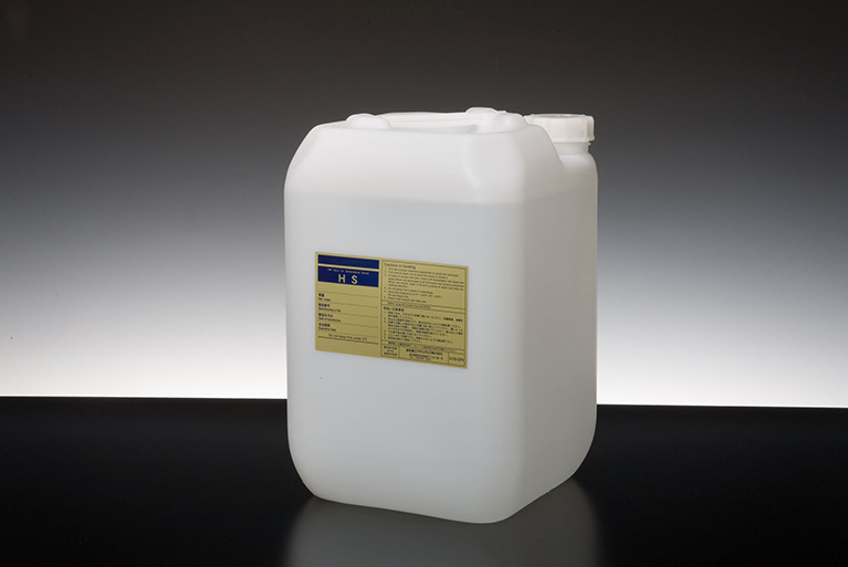
*1 CMP (chemical mechanical planarization) refers to technology for smoothing and flattening the rough surfaces created in the production process of semiconductor devices. CMP slurries consist of abrasive particles, additives and aqueous media used for surface treatment.
*2 Source: Global Net Corp.
*3 Semiconductor memory refers to an integrated circuit in a semiconductor device tasked with storing data.
*4 Semiconductor logic refers to an integrated circuit serving as a calculator in a semiconductor device.
*5 Source: Fuji Keizai Co., Ltd., “2022 Current Status and Future Prospects of the Semiconductor Materials Market.”
*6 Ceria slurry refers to a CMP slurry using abrasive cerium oxide particles to enable high-polishing rate with few scratches.
*7 Source: Global Net Corp.
*8 Nano-ceria slurry refers to a CMP slurry using fine abrasive particles measuring a few nanometers in diameter developed with Showa Denko Materials’ unique fine particle synthesis technology.
- Share: