ASIA ELECTRONICS INDUSTRYYOUR WINDOW TO SMART MANUFACTURING
New Techniques Aim at Diverse Soldering Methods
The soldering industry witnessed the drooping of the market amid the novel coronavirus (COVID-19) pandemic. However, the market conditions have begun to bounce back gradually signifying the recovery of the manufacturing industry in China.
Solder manufacturers have been accelerating the development of new products that meet diverse market needs. They are offering products tailored to different finished products, such as mobile devices, automotive electronics, and industrial equipment. They also meet the diversification of soldering methods, including the use of soldering robots, dip soldering, and dispensing of solder paste, as well as customers’ requirements that accompany the globalization of the soldering business. Solders are used in electronic and electric devices to electrically join circuits of printed circuit boards (PCBs) with electronic components and semiconductors mounted on electronic circuits.
Soldering Process
The joining process in soldering is achieved through wetting, melting and spreading of the base metal and solder after the removal of oxidized film by flux. The molten solder expands onto the surface of the metal from which oxidized film is removed (wetting), and then, the metal components of the base metal melts into solder component (melting). In the melting process of the metal component, an intermetallic compound is formed from the reciprocal migration of atoms from both the solder material and the base metal (spreading).
A solder metallic bond is achieved by melting and spreading. In particular, the wetting property significantly affects the functionality and safety of products, making it a crucial property of solders.
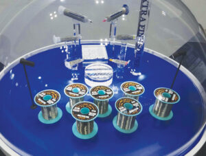
Diversifying Solder Composition
Solders are a kind of alloys. Conventionally, tin (Sn), copper (Cu), and lead (Pb)-based solder alloys were the mainstream. However, in consideration of the effects of lead on the environment, products, in which silver (Ag) is added to Sn and Cu, in place of Pb, are widely used today.
The Japan Electronics and Information Technology Industries Association (JEITA) recommended as standard in Japan since 2000 Sn-3Ag-0.5Cu (SAC305), which employs Sn and Cu as base materials and includes 3 percent Ag (mass ratio). Since then, SAC305 has been widely adopted in home electric appliances and audio-video (A/V) products.
Thereafter, rising Ag prices, increasingly higher density of PCBs, miniaturization of components mounted onto PCBs, and use of increasing number of electronic components in smartphones and automobiles, have led to the appearance of diverse solder products, which continue to evolve.
With the diversification of products in which solders are used, including smartphones and electric vehicles (EVs), solders that accommodate new products have been commercialized by adding new materials, such as indium (In), cobalt (Co), antimony (Sb), and germanium (Ge), to enhance the joining strength.
For example, KOKI Co., Ltd. has commercialized a solder paste, in which bismuth (Bi) and In have been added as reforming components to Sn and Ag being the base metals. Reforming elements melt into Sn and improve the strength of Sn crystal. Thus, the solder paste reduces the decrease in the connection strength and fracture of solder joints during cooling and heating cycles.
Nihon Almit Co., Ltd. has brought to market a flux-cored solder for automotive use with the addition of Bi, Sb, silicon (Si) and In with Sn, Ag, and Cu as base metals, responding to diverse needs. With products with low melting points (solid phase temperature: 194℃/liquid phase temperature: 206℃), the company has developed an alloy of Sn, Ag, Bi, and In. The company also offers an alloy of Sn, Ag, Cu, Bi+α as a high-strength solder and an alloy of Sn, Cu and nickel (Ni) as a product that prevents the erosion of soldering iron.
Reduction of Voids
Electrification of automobiles requires advanced technologies. PCBs mounted on automobiles require higher-quality soldering that withstands harsh environments, such as temperature, humidity, and vibrations. In particular, reduction of voids or air bubbles, which generate in the solder and cause defective soldering, is a crucial challenge.
Voids generate when solder melts and hardens. All kinds of efforts have been made to reduce voids. Vacuum reflow ovens are also attracting attention as they can suppress the generation of voids by providing a vacuum zone in the solder bath.
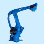
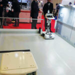
Soldering Robots
Soldering robots automate the soldering of PCBs, which has conventionally been carried out manually by workers. The demand for soldering robots has been expanding against the backdrop of the growing needs for the automation of production.
Mounting of components other than chip components, for example, large capacitors and connectors, have been done manually on PCBs after surface mounting, and partial soldering has been carried out manually by skilled workers. However, rising labor costs, shortage of skilled workers, and solving problems, such as human errors, have made soldering robots indispensable.
A soldering robot consists of the heating section, robot section, and controller section. Programming the robot enables automatic soldering of needed locations. Without using a solder bath, soldering robots can be installed anywhere where there is a table, power supply and dry air.
The heating section delivers the melting of solder through iron tip method, semiconductor laser method, and ultrasonic method. The iron tip method employs the same method as conventional soldering tip, and the soldering is automated.
The semiconductor laser method uses high-output semiconductor diode laser as the heat source to locally heat components to be mounted without contact and solder them. It can minimize the effects of heat to the periphery of the mounting position. In the ultrasonic method, soldering is performed by vibrating the iron tip with the width of several micron meters.
- Share: