ASIA ELECTRONICS INDUSTRYYOUR WINDOW TO SMART MANUFACTURING
Hitachi High-Tech Launches New Surface Inspection
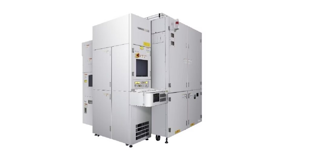
Hitachi High-Tech Corporation has introduced LS9600, a new system for detecting particles and defects on non-patterned wafer surfaces. Particularly, it features a new high-output, short-wavelength laser that improves throughput at the sensitivity levels required for the mass production of cutting-edge semiconductor devices.
Accordingly, the throughput is ~2.6 times compared to the company’s previous generation systems. By introducing this product, Hitachi High-Tech will continue to help to improve yields and reduce inspection costs associated with customers’ mass production of semiconductor devices.
Development Background
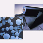
Non-patterned wafer inspection systems are used for applications such as controlling the condition (cleanliness) of non-patterned wafers to manage particles and defects in semiconductor device manufacturing equipment. Due to the shrinking of semiconductor devices, the defects of interest (DOIs), which impact yield during the manufacturing process, have also become smaller in size. For that reason, there is a growing need for high-sensitivity inspection that can detect DOIs of 20nm and smaller across the entire surface of non-patterned wafers. In addition, aside from high-sensitivity inspection to improve yield, there is also a strong demand for high throughput, which leads to lower inspection costs.
Key New Technologies
This system achieves both high sensitivity and high throughput by implementing the following new technologies.
High-Output, Short-Wavelength Laser
The deep-ultraviolet laser has a higher output and shorter wavelength than legacy systems, which increases the amount of light scattered by microscopic defects. Thus, achieving a higher degree of sensitivity.
New Optical Detection System
The new optical detection system features a larger surface area to capture light scattered by DOIs compared to the legacy systems. In addition, its newly developed high-sensitivity sensor has improved the detection rate of weak scattered light by around 20 percent.
New Data Processing System
Improved scattered light data-processing algorithms deliver higher sensitivity, together with higher throughput due to high-speed, real-time data processing. By using this product, Hitachi High-Tech is working to meet customers’ various needs in processing, measurement, and inspection throughout the semiconductor manufacturing process. Add to this, the company’s wafer optical inspection systems, and electron beam-based products such as a traditional CD-SEM*1 and DR-SEM*2
“We will continue to provide innovative and digitally enhanced solutions to our products for the upcoming technology challenges, and create new value together with our customers, as well as contributing to cutting-edge manufacturing,” the company said in a statement.
Notes:
*1CD-SEM (Critical Dimension-Scanning Electron Microscope): An equipment for measuring the microscopic circuit patterns on semiconductor wafers. Used for inspections on semiconductor devices development and production lines, these systems are essential for yield management.
*2DR-SEM (Defect Review-Scanning Electron Microscope): An equipment for reviewing the microscopic circuit patterns and defects on semiconductor wafers. Used for inspections on semiconductor devices development and production lines, these systems are essential for yield management.
- Share: