ASIA ELECTRONICS INDUSTRYYOUR WINDOW TO SMART MANUFACTURING
Latest Hybrid Placement Solution Merges Semi, SMT
Currently, end-to-end data communication, automation, and high-speed processing of dies are the greatest challenges facing the semiconductor industry.
Global technology leader for electronics manufacturing ASMPT, with its Semiconductor (SEMI) and SMT Solutions segments, presents intelligent and efficiency-enhancing solutions in SEMICON KOREA 2023. It highlights the solutions under the motto “Enabling the digital world” from Feb. 1 to 3 at booth D620 in hall D of SEMICON KOREA.
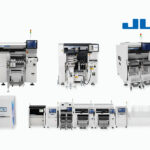
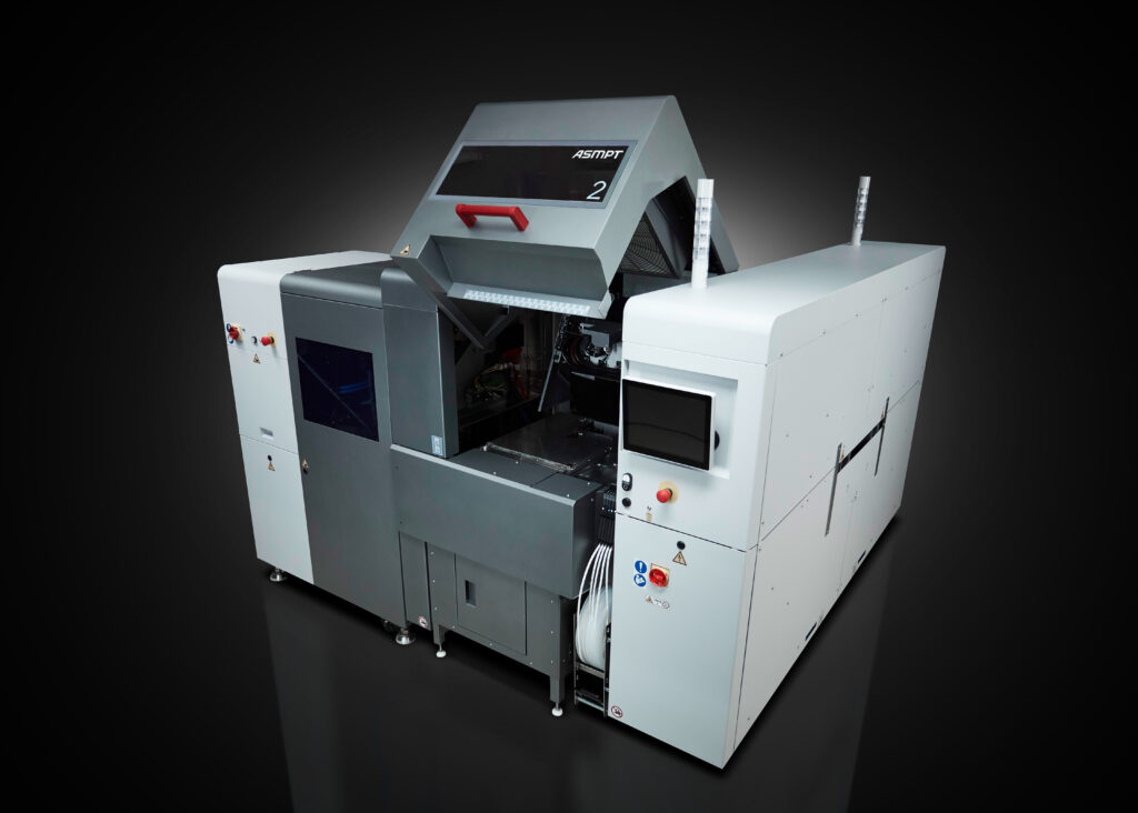
ASMPT showcases the new hybrid SIPLACE CA2 placement solution for the system-in-package (SiP) market. It combines the processing of surface-mount devices (SMDs) and dies directly from diced wafers in a single work step. By integrating the best of both worlds, the SIPLACE CA2 improves throughput in advanced packaging tremendously.
“By combining the SMT and semiconductor worlds with their respective strengths in a single machine, ASMPT revolutionizes the SiP production with its SIPLACE CA2,” declares DS Kim, general manager Korea with ASMPT.
Comprehensive Suite of Packaging & Assembly Solutions
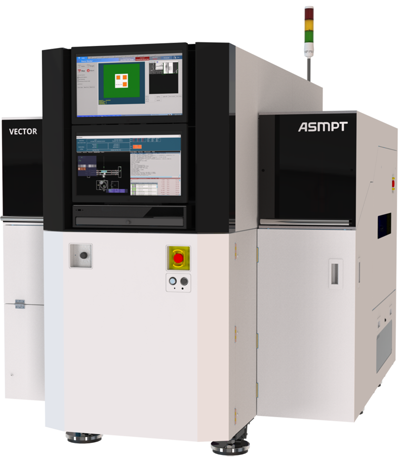
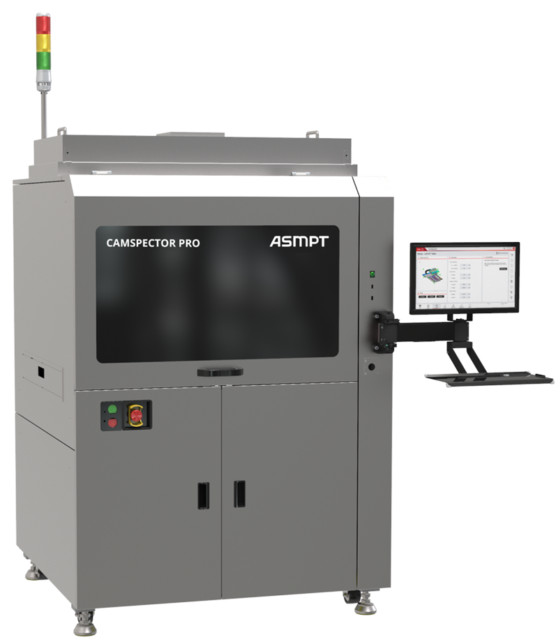
Meanwhile, targeting the power module and automotive market, ASMPT presents two other impressive machines. First is the POWER VECTOR component tacking tool for power modules and power-integrated modules (PIM). The second machine is the CamSpector Pro, the world’s first sub-micron AOI system with foreign materials (FM) cleaning. Thus, ASMPT offers the most comprehensive suite of packaging & assembly and SMT solutions for multiple end applications.
Advanced packaging is becoming ever more complex. At the same time, time and cost pressures are steadily increasing, and floor space is getting scarce and expensive. Meanwhile, production activities in the semiconductor field are divided into many individual and time-consuming processes carried out with expensive and slow special-purpose machines. As a result, seamless data communication or even smart automation is nearly impossible.
(Image source: ASMPT)
SMD, Die-Attach and Flip-Chip in a Single Work Step
The new SIPLACE CA2 processes SMDs and dies from a diced wafer in the same step. This hybrid machine handles up to 40,000 flip-chips, 50,000 chips in die-attach mode, and up to 75,000 SMDs per hour. More importantly, it does it all with a precision rating of up to 10μm @ 3σ. Thanks to its wafer exchange system, up to 50 different wafers can be used and exchanged in less than 6 seconds.
Also, as a specialty in the semiconductor field, the machine traces each die from which wafer it was taken, to where on the substrate it was finally placed. This process is called full single-die-level traceability. The ability to pick up dies directly from the diced wafer also eliminates the need for pre-taping them, which reduces costs dramatically and prevents mountains of waste.
Maximum Efficiency: Silver Sintering Process for Third-generation Semiconductors
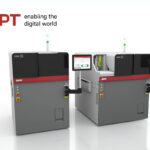
ASMPT also displayed solutions for smart automotive, power train, and power station applications. Specifically, the POWER VECTOR component tacking tool for power modules and power-integrated modules (PIMs) provides multi-chip bonding capabilities with high efficiency, high reliability, and high-temperature stability. Its flexible material handling enables die sizes from 0.5 to 16mm or even bigger on request and ultra-thin die handling. Also, it supports different silver sintering materials such as film stamping and pre-form. Moreover, the unique silver film quality inspection system ensures optimal silver coverage for perfect thermal and electrical conductivity.
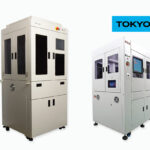
Top Quality: Unique AOI System for CMOS Modules
The CamSpector Pro is the first machine worldwide to provide sub-micron capabilities combined with a patented foreign materials (FM) cleaner. It assembles CMOS modules in both automotive and consumer electronics. The machine’s smart vision system detects contaminants down to 0.5μm. Additionally, it is configurable inline with other process equipment to enable fully automated, inline scalable production.
(Image source: ASMPT)
Best-in-class Equipment for Advanced Packaging
For advanced packaging applications, such as a fan-out solution, the SIPLACE TX micron was displayed. Also present was the new DEK TQ L high-speed solder paste printer with maximum speed and precision for large boards measuring up to 600 × 510mm. Moreover, the high-end Process Lens SPI system is also displayed. It controls and optimizes printing processes entirely on its own when combined with the WORKS Process Expert software.
“With all the industry-leading capabilities of ASMPT machines in combination with open and standardized interfaces and smart software solutions, we make it possible to integrate a multitude of processes in the advanced packaging field into ASMPT’s modular Open Automation concept for the “Integrated Smart Factory”. After all, ASMPT’s vision of “Enabling the digital world” also applies to the electronics manufacturing world of semiconductor and SMT,” says DS Kim.
- Share: