ASIA ELECTRONICS INDUSTRYYOUR WINDOW TO SMART MANUFACTURING
New Canon Wafer Measurement Tool Beefs up Lithography Systems
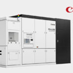
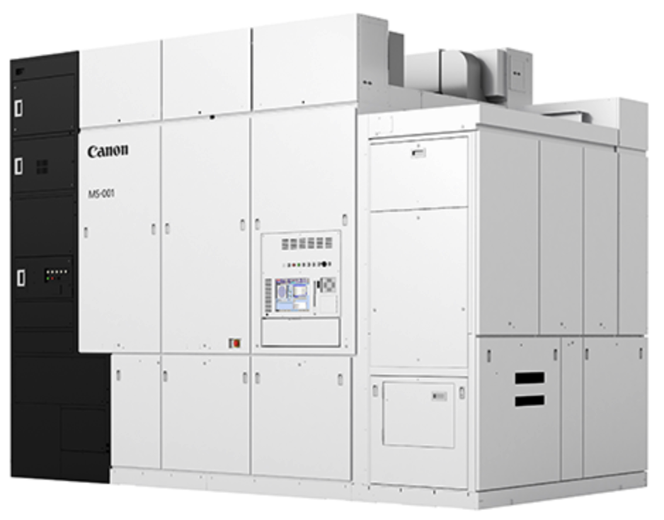
Canon Inc. announced the launch in Japan of the MS-001, a high-precision wafer alignment1 measurement device for semiconductor lithography systems.
In the manufacturing process of advanced semiconductors including logic and memory chips, the deformation of wafers is increasingly becoming an issue. This is due to the growing complexity of the manufacturing process. To manufacture semiconductor devices, wafer deformation must be measured accurately. This process overlays and exposes with high precision multiple layers of circuit patterns within a series of lithography systems.
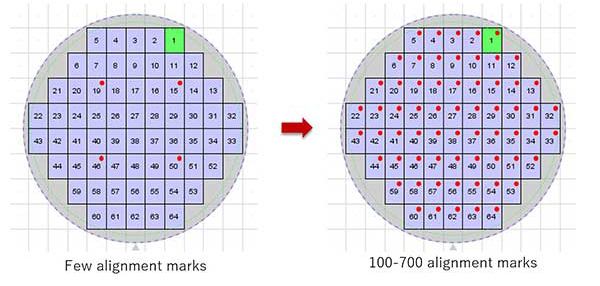
In the past, alignment marks on wafers are few. Nowadays in modern processes, they increased to hundreds to ensure the high accuracy required for overlay. Therefore, measuring hundreds of alignment marks results in significant time cost. Consequently, it reduces the productivity of the lithography systems.
Improves Productivity of Lithography System
The MS-001 wafer alignment measurement equipment allows the majority of alignment measurements performed in one batch process. They are done outside the lithography system before it receives the wafer. The wafer measurement equipment reduces the number of measurements performed inside them. Thus, it improves the productivity of the lithography system.
Canon’s MS-001 is equipped with an alignment scope that adopts an area sensor for multiple-pixel, low-noise imaging. Specifically, it measures even low-contrast alignment marks. Thus, it makes possible measurement of more types of alignment marks, which can be measured by conventional lithography systems. In addition, a newly developed light source for the alignment scope enables MS-001 to use 1.5 times the wavelength range of measurements2, giving users more freedom in selecting wavelength bands for measurement. Thus, MS-001 can measure alignment marks with higher accuracy than conventional semiconductor lithography systems.
Together with Canon’s Lithography Plus solution (released in Sept. 2022), users can aggregate operating status information from semiconductor lithography systems with data from the MS-001. By cross-referencing and monitoring MS-001 measurement data with other collected information using Lithography Plus, changes to the on-wafer alignment information can be detected. This allows automatic correction by the semiconductor lithography system. Utilizing Canon’s Lithography Plus solution, MS-001 also enables system owners to achieve centralized control of the alignment measurement and exposure processes, resulting in a reduced cost of ownership (CoO3).
1The process of detecting and measuring alignment marks on a silicon wafer for precise overlay of circuit patterns.
2Compared with the alignment scope of conventional Canon lithography systems.
3The sum of costs incurred from owning and operating equipment.
- Share: