ASIA ELECTRONICS INDUSTRYYOUR WINDOW TO SMART MANUFACTURING
Canon New Lithography System Suits Full-Frame Device Production
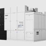
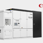
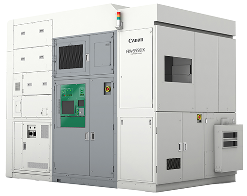
Canon Inc. announced the FPA-5550iX i-line stepper1 semiconductor lithography system for front-end processes. The new lithography system realizes a large exposure field of 50×50mm and a high resolution of 0.5µm2.
Suitable for High-Precision Device Manufacturing
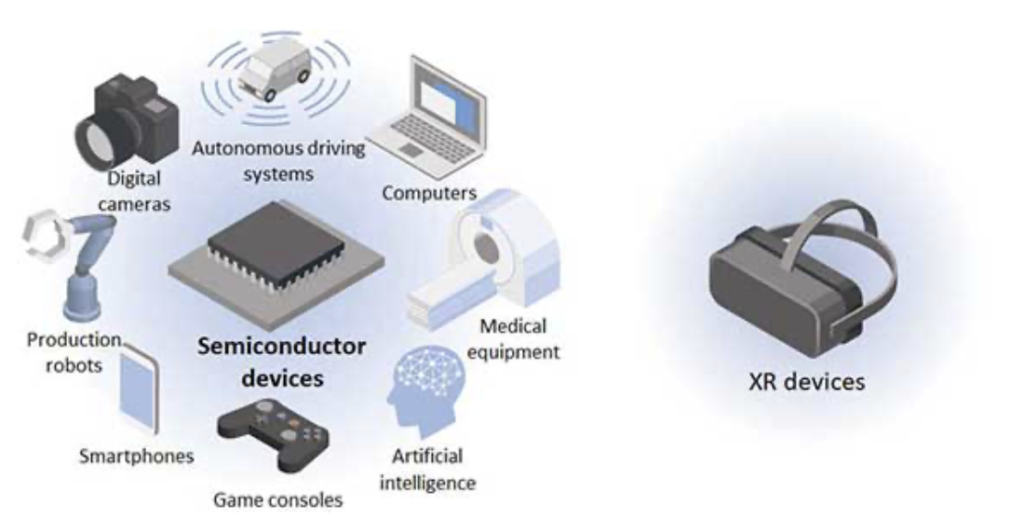
The FPA-5550iX lithography system’s large exposure field of 50×50mm and a high resolution of 0.5µm makes possible single exposure of a large field with high resolution. Specifically, this quality is necessary to produce full-frame CMOS sensors and other devices, in which higher precision is advancing. The new system is also capable of manufacturing small displays for such devices as head-mounted displays. Also, it enables the high-resolution single exposure required for manufacturing high-contrast micro-OLED panels3 with wide viewing angles, which are expected to grow as displays for cutting-edge XR devices. In addition to semiconductor devices, the new FPA-5550iX can also manufacture displays for cutting-edge XR devices. It thus supports the manufacture of a wide range of devices.
Specifically, FPA-5550iX utilizes the same projection lens used by its predecessor model, FPA-5510iX, which enables a high resolution of 0.5µm. Thanks to a wide exposure field, the system can perform high-resolution single exposure for full-frame CMOS sensors, next-generation displays for XR devices, and more. Moreover, manufacturing processes have been refined to ensure high-quality, stable production of projection lenses, many of which are used in the system. This aims to meet the strong demand expected for semiconductor lithography systems.
In addition, a new alignment scope that reads wider variety of alignment marks4 expands the range of processes in which FPA-5550iX is can be used. In addition to the “bright-field detection” function for measuring direct light, a new “dark-field detection” function was added to the alignment scope. This enables measuring of scattered and diffracted light, thus allowing users to select a wide range of measurement methods.
Moreover, it made possible low-noise measurement by expanding the range of usable wavelengths while also employing an area sensor for multi-pixel measurement. Thanks to these advancements, the system detects and measures low-contrast alignment marks. Additionally, the system optionally selects an infrared wavelength that can pass through silicon. Thus, it enables users to measure the alignment on the back of the wafer. This function is a requirement for the manufacture of back-illuminated sensors. The flexibility of alignment mark measurement thus allows the system to be utilized in a variety of processes.
When combined with Canon’s Lithography Plus solution platform (released in September 2022), FPA-5550iX provides operators with the ability to monitor the condition of the lithography system. It also performs analyses, helping them maintain appropriate quality control and higher utilization rates.
1A semiconductor lithography system that utilizes a 365nm wavelength mercury lamp as the light source. 1nm (nanometer) is 1 billionth of a meter.
21 micrometer=1/1,000,000 meter
3A production method for ultra-high resolution displays, made with silicon wafers featuring image quality characteristic to OLED
4Marks placed on silicon wafers to secure accurate circuit pattern overlay
- Share: