ASIA ELECTRONICS INDUSTRYYOUR WINDOW TO SMART MANUFACTURING
Rapidus to Start Construction of Advanced IC Facility
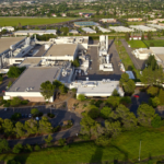
Rapidus Corporation said it will start preparing for the construction of a plant for the development and manufacturing of state-of-the-art semiconductors in Chitose City in Hokkaido. The Japan-headquartered company has been involved in the research, development, design, manufacture, and sales of advanced logic semiconductors.
Recently, the Ministry of Economy, Trade, and Industry (METI) and the New Energy and Industrial Technology Development Organization (NEDO) gave green light on the R&D project*1 as well as the plan and budget for FY2023. Thus, Rapidus will begin working in collaboration with local governments and related businesses.
Strengthens Collaborations
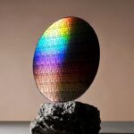
Rapidus has also started dispatching its researchers to the Albany Nanotech complex in New York, one of the world’s most advanced semiconductor research facilities. Particularly, they begun research and development in collaboration with IBM. Through these measures, it will develop 2nm node technology, build a short TAT pilot line in Japan, and conduct verification tests using test chips.
Through international collaboration with IBM, imec, and other entities, Rapidus will promote the development of advanced logic semiconductor technology and construct its state-of-the-art plant in Chitose City, and once the research period is concluded, it will aim to commercialize the results as an advanced logic foundry.
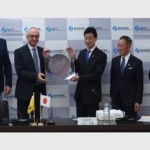
Last year, IBM and Rapidus forged joint development partnership to advance logic scaling technology. Primarily, the partnership has given a boost to Japan’s initiatives to become a global leader in semiconductor research, development, and manufacturing.
As part of this agreement, Rapidus and IBM will further develop IBM’s breakthrough 2nm node technology for implementation by Rapidus at its fab in Japan. This work will leverage IBM’s decades of expertise in semiconductor research and design.
Recently, Imec and Rapidus have agreed to set up a long-term and sustainable collaboration on advanced semiconductor technologies.
Note
*1 NEDO commissioned the project as part of the “Post 5G Information and Communication Systems Infrastructure Enhancement R&D Project/Development of Advanced Semiconductor Manufacturing Technology/R&D of 2nm-generation semiconductor integration technology and short TAT manufacturing technology based on Japan-US collaboration”
- Share: