ASIA ELECTRONICS INDUSTRYYOUR WINDOW TO SMART MANUFACTURING
EUV Ecosystem Poised to Rise in Korea
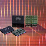
The world’s two largest memory chipmakers — Samsung Electronics and SK hynix — are rapidly adopting next generation of photolithography extreme ultraviolet technology (EUV). Meanwhile, chip making equipment makers and raw materials makers are flocking to Korea to create an EUV ecosystem.
EUV Suits Finer Chip Geometry
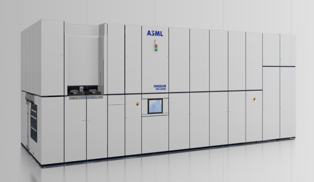
EUV is a disruptive lithography technology that uses EUV as light source to draw circuitry pattern on a wafer. The EUV light source is a far cry from the conventional ArF, as its shortest ever wavelength is 13.5nm.
As the chip circuitry width depends on the wavelength of the light source, the EUV is an inevitable technology enabler in attaining below 10nm circuitry patterns.
Yet, the technology is so disruptive that it requires totally different resources, tools and peripherals from those of the ArF equipment. For example, it uses tons of electrical power to power scanner, laser-driven tin plasma light source generation, and reflective optics tools, and optical mirrors.
As all matters and tools absorb EUV radiation, it also requires peripherals of different matters like photo resist, photo masks, blank masks, reticles, and pellicles.
This helps explain why there must be EUV-exclusive ecosystem.
Creation of EUV Ecosystem
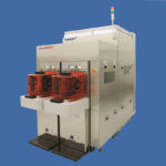
Leading the EUV ecosystem creation is ASML, a Dutch EUV photolithography equipment maker. The EUV equipment maker has agreed to establish its EUV cluster in Korea’s Hwaseung City, home to Samsung Electronics foundry chipmaking business, to construct a training and reproduction center to support Korean chipmakers.
When it comes to EUV photo resist, JSR, Shin-Etsu Chemical, Tokyooka Industrial (TOK) and Sumitomo Chemical of Japan are presently supplying them to Samsung and SK hynix. Meanwhile newcomers, like SK Materials, Dongjin SemiChem, Young Chang Chemical, and Samsung SDI of Korea set out to develop an EUV photo resist, Dupont of the U.S. plans to build EUV photo resist production facilities in Korea as an EUV ecosystem partner.
TOK of Japan is expanding its production capacity for EUV photo resist at its Incheon, Korea facility to meet surging demand.
S&S Tech of Korea is creating a manufacturing ecosystem from EUV blank mask to EUV photo resist to EUV photo mask and pellicles.
Esol of Korea has also completed developments of EUV photo resist test equipment.
In terms of EUV photo masks and bland masks, the likes of Hoya and Asahi Glass of Japan dominate the market.
FST of Korea is also working hard to develop EUV pellicles, while carrying out research & development projects to develop EUV pellicle inspection equipment and EUV photo mask pod equipment.
- Share: