ASIA ELECTRONICS INDUSTRYYOUR WINDOW TO SMART MANUFACTURING
Ansys Solutions Earn Samsung 2nm Process Nod
Following close collaboration with Samsung Foundry, Ansys has achieved certification of Ansys RedHawk-SC and Ansys Totem power integrity signoff solutions for Samsung’s latest 2nm silicon process technology.
Accordingly, the certification of these industry-leading electronic design automation (EDA) tools will lend confidence to early adopters of Samsung’s technology. Thus, creating leading-edge integrated circuits (ICs) in high-performance computing (HPC), smartphones, artificial intelligence accelerators, data center communication, and graphics processors.
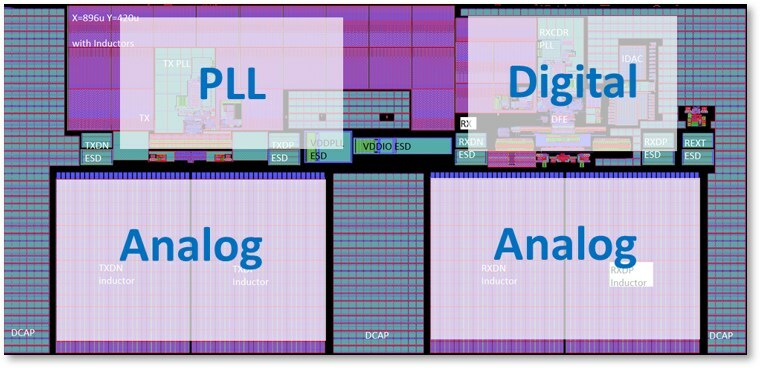
Samsung’s 2nm process is its third generation of gate-all-around (GAA) process technologies and continues the rapid progression of Moore’s Law using novel transistor devices for higher integration density, faster performance, and lower power. Meanwhile, RedHawk-SC provides industry-recognized signoff verification for electromigration (EM) and voltage drop (IR drop) on power distribution networks for digital designs. Totem provides similar checking for custom analog and mixed-signal designs.
Address New Customer Challenges
The predictive accuracy of Redhawk-SC and Totem has been verified through extensive testing as part of Samsung Foundry’s certification process. These products are part of the broad array of multiphysics analysis and simulation products offered by Ansys to support the growing scale and complexity of modern chip, 3D-IC, and electronic system designs.
“Samsung Foundry has traditionally worked very closely with Ansys to ensure that our mutual customers have timely access to the design tools they need to make the best possible use of Samsung’s technology potential,” said Sangyun Kim, vice president of Foundry Design Technology Team at Samsung Electronics.
In addition, Kim said, “We continue to expand the areas of collaboration with Ansys to address new customer challenges in leading digital, full-custom, mixed-signal, and 3D-IC designs.”
On the other hand, John Lee, vice president and general manager of the electronics, semiconductor, and optics business unit at Ansys, said, “Ansys and Samsung focused on delivering technology enablement solutions that meet our customers’ needs on the leading edge of silicon technology.” “This collaboration with Samsung Foundry makes the signoff fidelity of our Ansys multiphysics platform possible. At the same time, Ansys remains committed to powering the best user experience for our joint customers.”
- Share: