ASIA ELECTRONICS INDUSTRYYOUR WINDOW TO SMART MANUFACTURING
New Wafer Manufacturing Platform Tackles Chipmaking Challenges
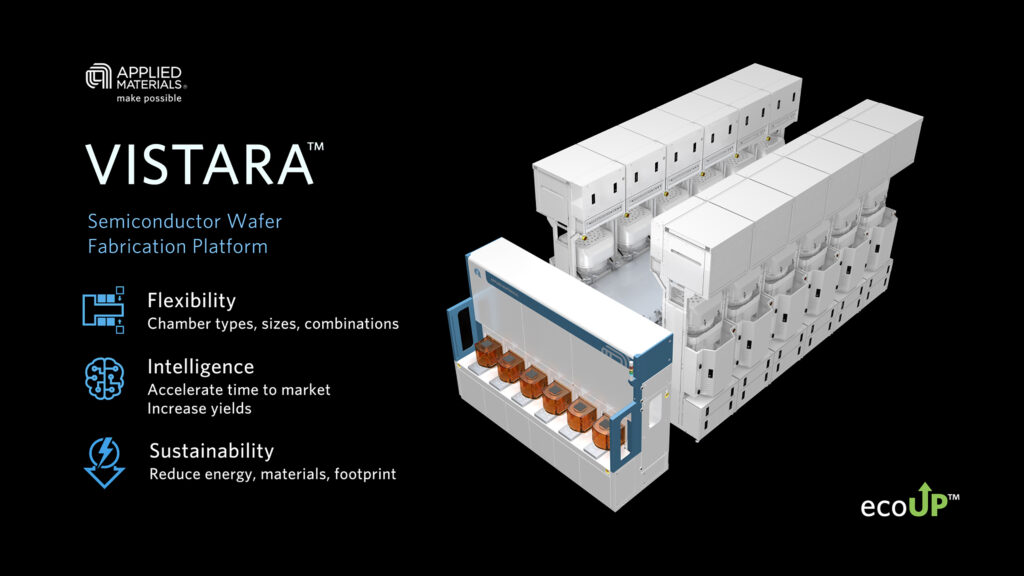
Applied Materials, Inc. has introduced Vistara™, its most significant wafer manufacturing platform innovation in more than a decade. The new platform was designed to provide chipmakers with the flexibility, intelligence, and sustainability needed to tackle growing chipmaking challenges.
The Vistara platform builds upon the company’s long history of leadership in semiconductor manufacturing platforms that include Endura®, Producer®, Centura® and Centris®, found in fabs around the world and used in the production of virtually every chip made. Specifically, Vistara was developed over more than four years by hundreds of engineers from across Applied’s hardware, software, process technology and ecoefficiency design teams.
“Like its predecessors, Vistara is designed to be a trusted platform for many years of customer innovation, reliability and productivity,” said Dr. Prabu Raja, President of the Semiconductor Products Group at Applied Materials. “Vistara is being launched at an opportune time when the semiconductor industry needs unique solutions to address growing chipmaking challenges related to complexity, cost, cadence and carbon emissions.”
Flexibility
Vistara’s unmatched flexibility helps chipmakers solve the growing complexity challenges of advanced chipmaking. The Vistara platform can use an unprecedented wide variety of chamber types, sizes and configurations from Applied and its partners. It can be configured with four or six wafer batch load ports and from as few as four to as many as 12 process chambers to address a wide variety of workloads. The platform accepts both smaller chambers used in processes like atomic layer deposition and chemical vapor deposition. Moreover, it accommodates larger chambers used in processes such as epitaxy and etching.
Applied and its customers can combine these chambers to develop IMS™ (Integrated Materials Solution®) recipes. In IMS, a number of sequential wafer manufacturing process steps are completed in the same system under vacuum. The flexibility of Vistara gives chipmakers IMS technology combinations that were never possible before. This enables them to deliver innovative transistors, memories and wiring, improve performance and power, and protect against yield-killing particles and defects.
Intelligence
The Vistara platform’s intelligence helps customers address growing cadence and cost challenges. Accordingly, it accelerated time to market and maximized productivity and yield in high-volume manufacturing. Also, Vistara platforms are configured with thousands of sensors that feed massive, real-time data to Applied’s AIx™ software platform. Specifically, the platform offers applications spanning R&D, process transfer and ramp, and high-volume manufacturing. Actionable data from thousands of process variables enables engineers to use the power of machine learning and AI to accelerate recipes that can result in the best chip performance and power and widest process windows.
Intelligence is incorporated throughout the platform. This includes the factory interface module where load locks are intelligently controlled to optimize pump and vent times. Thus, it helps chipmakers reduce particles and defects to maximize yields. Platform robots are automatically calibrated to reduce start-up times by as much as 75 percent. In production, the Vistara platform continuously monitors and calibrates its components to minimize manual intervention, maximize uptime and predict maintenance needs.
Sustainability
The increase in semiconductor process complexity and steps adds to the energy and materials needed to produce each wafer. Vistara is the first platform purpose-built to advance Applied’s “3×30” initiative. Specifically, it aims to achieve 30-percent reductions in equivalent energy use, the impact of chemical use, and cleanroom floorspace requirements, all by 2030. Engineers completely redesigned the Vistara platform’s gas panels to reduce the equivalent energy consumption by more than 50 percent compared to the previous design. Also, they optimized the way the platform uses energy-intensive sub-fab components including pumps, heat exchangers and chillers.
Mainly, these improvements can lower platform energy consumption by as much as 35 percent compared to previous platforms. Thus, it helps chipmakers reduce their Scope 1 and Scope 2 emissions. Vistara also reduces the cleanroom footprint of a system by as much as 30 percent. Such savings help customers generate more wafers in smaller facilities. Thus, it reduces the use of carbon-intensive construction materials such as concrete and steel. Specifically, a 30-percent reduction can potentially save 1 million metric tons of carbon for every 100K wafer-starts-per-month (WSPM) fab built.
Introducing EcoTwin™ Software
Further, Applied also introduced EcoTwin eco-efficiency software, available first with the Vistara platform. EcoTwin software uses sensor data to help engineers monitor the real-time energy and chemical consumption of chambers, systems, and subfab components. Process engineers can use the EcoTwin dashboard to compare the carbon impact of alternative chemicals, recipes and production techniques. This process continuously improves sustainability over the life of a node and track and report on progress toward sustainability goals.
The first Vistara platforms are being shipped to all leading memory customers for use in etch applications. Applied expects unit growth across its major platforms as the wafer fab equipment industry grows to support projected increases in worldwide semiconductor demand.
- Share: