ASIA ELECTRONICS INDUSTRYYOUR WINDOW TO SMART MANUFACTURING
New Technologies Boost Chip Design, Integration
Applied Materials, Inc. has introduced new technologies and capabilities designed to help its customers accelerate their technology roadmaps for heterogeneous chip design and integration. The company combines its technologies in advanced packaging and large-area substrates with industry collaborations to speed the availability of solutions.
This aims to deliver simultaneous improvements in power, performance, area, cost, and time to market (PPACt).
Heterogeneous integration brings new kinds of design and manufacturing flexibility to semiconductor and system companies. It allows integration of chips of various technologies, functions, and sizes in one package.
Applied Materials supplies advanced packaging technologies with optimized products spanning etch, physical vapor deposition (PVD), chemical vapor deposition (CVD), electroplating, surface treatments and annealing. The company’s Advanced Packaging Development Center in Singapore houses broadest portfolio of products. These enable the foundational building blocks of heterogeneous integration, including advanced bump and micro-bump, fine-line redistribution layer (RDL), TSV and hybrid bonding.
“Applied’s industry-leading portfolio of advanced packaging solutions gives customers the broadest selection of enabling technologies for heterogenous integration,” said Nirmalya Maity, Corporate Vice President of Advanced Packaging at Applied Materials. “…We are building an ecosystem that can accelerate our customers’ PPACt roadmaps and create exciting new growth opportunities for Applied.”
Today, Applied Materials is unveiling innovations in three areas critical to advanced packaging for heterogeneous integration. These areas are die-to-wafer hybrid bonding, wafer-to-wafer bonding and advanced substrates.
Accelerating Die-to-Wafer Hybrid Bonding
Die-to-wafer hybrid bonding uses direct, copper-to-copper interconnects to increase I/O density and shorten the wiring length between chiplets to improve overall performance, power, and cost. To accelerate development of this technology, Applied is adding advanced software modeling and simulation to its Advanced Packaging Development Center. This builds upon the joint development agreement announced in October 2020 between Applied Materials and BE Semiconductor Industries N.V. (Besi) to develop the complete and proven equipment solution for die-based hybrid bonding.
“Our joint development program with Applied Materials has greatly enhanced our combined understanding of the co-optimized equipment solutions necessary for customers to utilize complex hybrid bonding processes in wafer level production environments,” said Ruurd Boomsma, Besi’s Chief Technology Officer.
For Wafer-to-Wafer Hybrid Bonding
Wafer-to-wafer bonding enables chipmakers to build certain chip structures on one wafer and others on a second wafer and then bond the wafers to create complete devices. To achieve high performance and yield, the quality of the front-end processing steps is critical as is the precise uniformity and alignment of the wafers as they are being bonded. Applied today announced a joint development agreement with EV Group (EVG) to develop co-optimized solutions for wafer-to-wafer bonding. The collaboration brings together Applied Material’s semiconductor process expertise in deposition, planarization, implant, metrology and inspection with EVG’s leadership in wafer bonding, wafer pre-treatment and activation, as well as alignment and bond overlay metrology.
“Semiconductor innovation is increasingly being fueled by 3D integration and engineered materials, which drive greater demand for wafer-to-wafer hybrid bonding. Optimizing this critical process for new applications requires an in-depth understanding of integration issues both up and down the process chain,” said Dr. Thomas Uhrmann, Business Development Director at EVG.
“Through collaborations with industry partners including Besi and EVG, Applied Materials is providing our customers the capabilities and expertise they need to accelerate development and adoption of hybrid bonding technologies, both die-to-wafer and wafer-to-wafer,” said Vincent DiCaprio, Managing Director of Business Development for Advanced Packaging at Applied Materials.
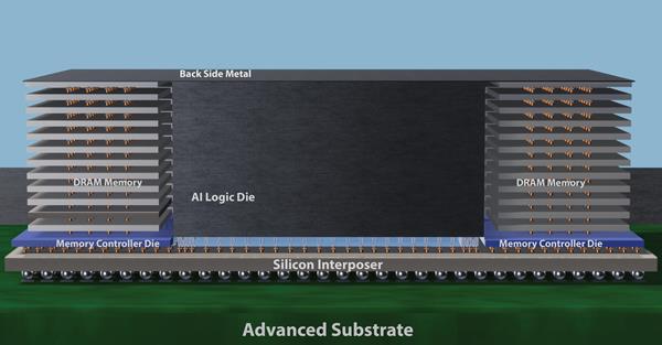
Larger, More Advanced Substrates Deliver PPAC Benefits
The need for more advanced substrates is increasing as chipmakers squeeze greater numbers of chips into sophisticated 2.5D and 3D package designs. To enable larger package sizes with greater interconnect density, Applied Materials is using state-of-the-art panel-level processing technology from its recent acquisition of Tango Systems. Panel-size substrates, which can measure 500×500mm or larger, can accommodate a greater number of packages compared to wafer-size formats. They provide a cost benefit in addition to better power, performance, and area.
As its customers adopt these larger panel sizes, Applied Materials is providing them with access to large-area materials engineering technologies from its Display Group. These include deposition, eBeam testing, SEM review and metrology, and focused ion beam for defect analysis.
- Share: