ASIA ELECTRONICS INDUSTRYYOUR WINDOW TO SMART MANUFACTURING
Applied Materials to Extend Leadership in Chip Manufacturing Technology
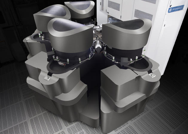
Applied Materials, Inc. said it intend to make multi-billion-dollar investments in its innovation infrastructure in the United States. Additionally, it will expand its global manufacturing capacity between now and 2030. These investments will enhance customer collaboration to accelerate improvements in semiconductor performance, power and cost. Moreover, they will enable the company to increase equipment manufacturing capacity as the digital transformation of the economy creates the opportunity for a $1 trillion semiconductor market.
“Applied Materials is the world leader in materials engineering solutions – the foundational technologies that define how current and future generations of chips are made,” said Gary Dickerson, President and CEO. “With these investments, we will double our innovation infrastructure in the United States. It will also significantly expand our ability to serve customers building new fabs in America and around the world.”
Next-Generation R&D Center
At the heart of these investments, Applied Materials plans to build a next-generation R&D center in Sunnyvale, California. This high-velocity innovation platform will be dedicated to advancing materials engineering, foundational chip technologies and process equipment. The Silicon Valley center will play a central role in collaborative R&D with all major chipmakers. It will bolster university partnerships and be capable of engaging with a future U.S. National Semiconductor Technology Center.
Applied expects to make this investment with support from the U.S. government. The CHIPS and Science Act and the State of California through the Governor’s Office of Business and Economic Development (GO-Biz) California Competes Grant awarded earlier this year are expected to give provisions. An event to mark the launch of this investment is planned for early 2023 in Silicon Valley.
In addition, Applied Materials intends to expand its U.S. equipment manufacturing capacity. It will invest in new infrastructure to both accelerate collaboration with the industry ecosystem. Also, it will develop the talented workforce needed to build America’s strength in critical future technologies. The investment in manufacturing capacity will expand the company’s factories in Austin, Texas which has been the home of Applied’s volume-manufacturing operations since 1993.
“Applied Materials has deep core capabilities in the U.S. – from our research centers in California and New York, to our factories in Texas and our product operations in Massachusetts and Montana,” said Dickerson. “No other semiconductor equipment company has a comparable footprint in the U.S. We intend to invest boldly and build on this world-class infrastructure to accelerate our technology leadership and enable our customers’ growth for decades to come.”
Applied is also investing in its global infrastructure. Specifically, it holds a groundbreaking ceremony for an expansion of its regional hub in Singapore. Together with the planned expansion in the U.S., it will significantly increase Applied Materials’ capacity to serve growing worldwide demand for semiconductors.
- Share: