ASIA ELECTRONICS INDUSTRYYOUR WINDOW TO SMART MANUFACTURING
Toray’s New Carbon Paste to Revolutionize Micro-Mounting
Toray Industries, Inc. recently developed a material that can bond micro-electronic components at temperatures more than 30°C lower than with existing technologies. That is less than half their levels and under low-pressure conditions. Mainly, the company achieved this breakthrough by integrating adhesion technology with its RAYBRID® photodefinable conductive material. Accordingly, it is developing this material for wiring in electronic components, touch sensors, and other applications.
The company plans to start mass production of the bond material in early 2025. Specifically, RAYBRID is a photodefinable functional material incorporating dispersed metals and other conductive particles and glass, ceramics, and other insulating particles.
Solder, a common bonding material, and other alloys are unsuitable for high-speed mounting. That is because miniaturization of bumps is hard while mounting necessitates high temperatures and pressure. This has become a significant mass production issue because of challenges with micro-LED displays. In particular, this emerging display technology requires large-volume, high-speed mounting of LED chips just 10 to 20µm large.
To this end, Toray developed a photodefinable carbon paste. Specifically, it combined proprietary nano-carbon dispersion technology with photodefinable conductive paste technology incorporating silver and other metallic particles that it has amassed over the years. The carbon enhances reliability, enabling bonding with wiring across diverse applications.
Details of New Technology
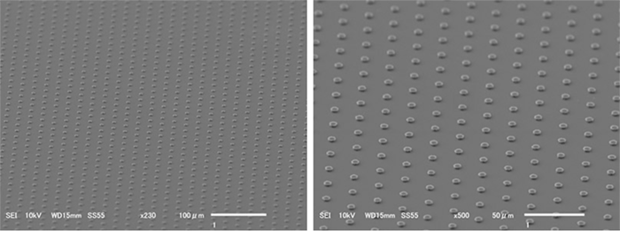
1. Fine bump formation
Toray’s new bonding material uses photolithography to form bumps with diameters as small as 5µm (Figure 1). This is a significant improvement over the 30µm diameter limit with conventional materials, enabling micro-mounting of micro-LEDs and semiconductors.
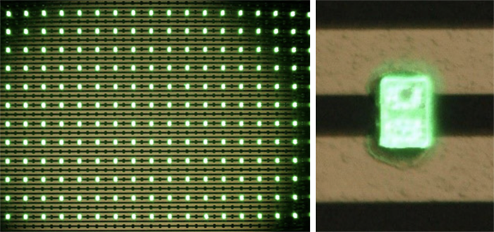
2. Large-area batch mounting with bonding at low temperatures and pressure
Toray’s unique organic design slashed the required temperature by 70°C, to 110°C, while halving the pressure needed to 5 megapascals. This enables batch mounting of micro-LEDs and significantly increases productivity (Figure 2).
3. Inspection and repair technology
Repairs are necessary for electronic components if they do not light after mounting. It is impossible with conventional technology to re-form bumps in unlit areas. Repairs have thus been a mass-production challenge. Toray’s material makes it possible to laser-transfer bumps to other substrates, re-forming bumps on repair locations.
The company employed the mounting and laser transfer facilities of Toray Engineering Co., Ltd., to verify large-area batch mounting and repair technology.
Toray has built a robust mass production and supply structure in developing photodefinable conductive materials for electronic components, displays, touch sensors, and other applications over the past two decades. It will leverage its new bonding material to broaden its materials lineup and expand its business in micro-LEDs, semiconductors, and other new fields.
Toray will keep leveraging core technologies in organic chemistry, polymer chemistry, biotechnology, and nanotechnology to undertake R&D and conceive innovative materials that drive fundamental social change. In so doing, it will endeavor to materialize its corporate philosophy of contributing to society by creating new value through innovative ideas, technologies, and products.
- Share: