ASIA ELECTRONICS INDUSTRYYOUR WINDOW TO SMART MANUFACTURING
New Material Simplifies Bonding, Propels MicroLED
Toray Industries, Inc. has developed a laser transfer release material to swiftly arrange light-emitting diode (LED) chips. Developed in collaboration with its subsidiary Toray Engineering Co., Ltd., the new materials simplify bonding between LEDs and wiring and a substrate side wire material that helps enlarge displays. In addition, the new material is also vital for creating microLED displays and enhancing their performance.
The Toray Group looks to contribute to microLED display progress for the diverse material and equipment for the fabrication and inspection.
Accelerates MicroLED Production
MicroLED displays offer tremendous potential for their outstanding performance and small environmental footprints. Moreover, these advanced devices offer exceptional brightness, color gamut, contrast, and reliability. In addition, their power consumption is low because of the high luminous efficiency of their LEDs.
The challenge has been to come up with technology to swiftly achieve regular arrangements of numerous microLED chips and reduce fabrication costs to sufficiently drive their widespread adoption. The new laser transfer material enables fast placement of numerous LED chips in any position on a substrate in the display manufacturing process.
Using this material with Toray Engineering’s laser transfer and inspection equipment can accelerate microLED production. It also creates displays free of color irregularities through selective placement that reflects the color tone of each LED chip.
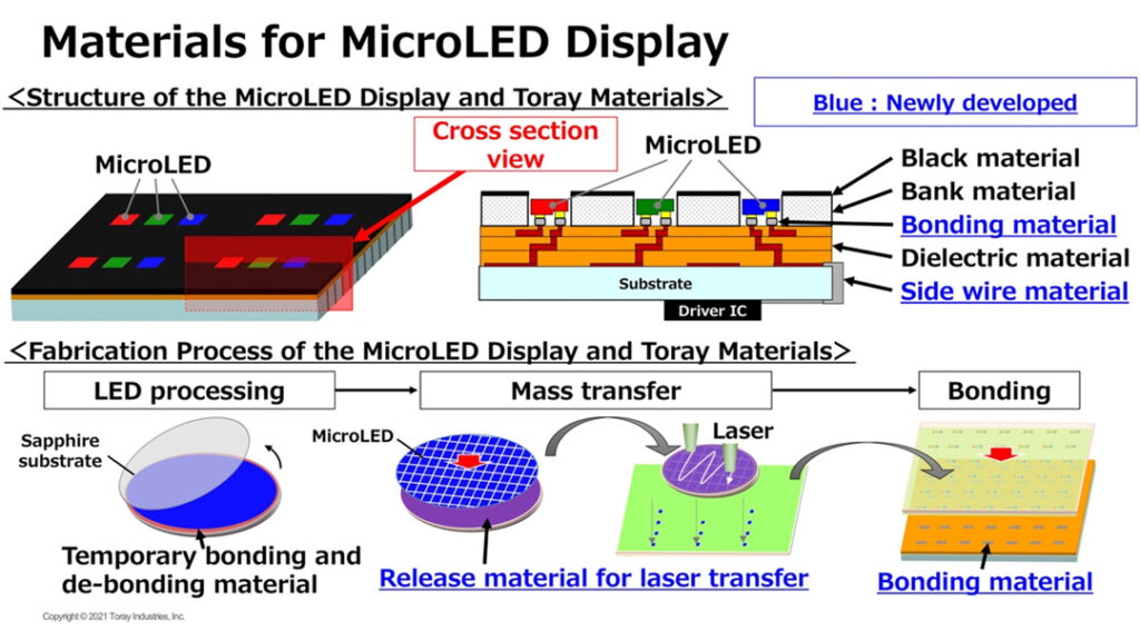
The new bonding and substrate side wire materials are the fruit of further work on RAYBRID®, a proprietary photosensitive conductive material.
The material that connects LED chip electrodes to metal trace on the substrate enables faster joint formation at lower temperatures. Moreover, it also lowers bonding force compared to the conventional connection methods. Because of this, it is easier to replace defective LED chips, which has been a challenge to date, and helps improve yields during manufacturing.
The substrate side wire material transmits signals from the surface to the back of a substrate. This simplifies the wiring formation process and makes it possible to seamlessly line up and enlarge multiple displays.
Deliver Products With New Value
Toray has already mass-fabricated microLED display materials. They include dielectric materials for wiring LED chips, black materials for enhancing display blackness to achieve high contrast, and temporary bonding and de-bonding materials for thinning or peeling off LED chip substrates. It aims to augment its lineup with bank materials for more colors and exceptional brightness.
Toray accordingly seeks to broaden its lineup of materials for microLED displays. Consequently, the goal is to combine them with Toray Engineering’s fabrication and inspection equipment. Ultimately, this is to offer total solutions for microLED display manufacturing and contribute to mass fabrication of microLED displays.
Toray said it will continue leveraging its core technologies of synthetic organic and polymer chemistry, biotechnology, and nanotechnology. They will use this edge to research and develop advanced materials and deliver products with new value.
- Share: