ASIA ELECTRONICS INDUSTRYYOUR WINDOW TO SMART MANUFACTURING
Eliyan’s Interconnect Solution Propels Generative AI
Generative artificial intelligence (AI) has emerged from the laboratory to seize the public’s attention. Less attention goes to the foundational challenge of AI: its need for massive computational and memory resources.
There is a growing struggle between the complexity of AI models—spiraling—and the resources available—growing slowly. At the root of this growth struggle lies a technology hardly discussed at all outside technical circles. These are the multi-die packaging and the accompanying “chiplet” approach, and the interconnect between dies that ultimately determines the scale, performance, and energy consumption of the hardware that executes the AI models.
Huge Models, Huge Chips
The scale of the software models that underlie generative AI is unimaginable. Estimates vary wildly, but it has been reported that GPT-4 has over a trillion parameters. Each of which has to be trained using a petabyte of input data, at a cost of about US$10 billion. Furthermore, each time the model is run by a user, many of those trillion or so parameters are used in multiplication calculations—another huge workload that goes on day in and day out. The cost is not just cash, but power, carbon emissions, and cooling water.
Traditionally, the computer industry has responded to performance and power challenges by summoning up Moore’s Law—let’s just use a bigger chip. This thinking has led the migration of generative AI models from giant datacenter CPUs to even bigger GPUs and to huge application-specific AI accelerator chips. But this solution is failing.
Successive process generations offer more transistors per square millimeter, but not necessarily faster circuits or more energy-efficient ones. Also, today’s GPUs and accelerator ASICs have reached the maximum die size allowable by the semiconductor manufacturing equipment. As such, it has been physically not possible to build bigger dies that currently available at present.
A further problem is presented by AI applications’ hunger for memory bandwidth. That means the performance of the application depends on having enormous amounts of fast memory—remember those trillion parameters—inside or very close to the computing chips.
The Multi-Die Path
It could have been easier to put multiple chips together on a circuit board. However, the electronic connections between the IC packages impose serious speed limits and consume excessive power. A board-level solution can’t deliver the performance or energy efficiency the industry needs.
Another solution is available: putting multiple dies within millimeters of each other on a single substrate, inside one package. This is multi-die packaging. It has been used in highly demanding and highly expensive systems such as military radars for years. Nonetheless, recently, multi-die packaging has converged with another idea: chiplets.
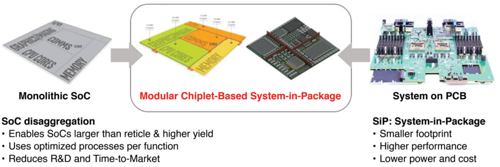
The idea is to replicate the rich open market that exists for packaged ICs, but for bare dies to go into multi-die packages. By defining standard interfaces between dies of different kinds—much like the PCIe bus at board level—and investing in an infrastructure for designing, building, and testing multi-die assemblies, the industry hopes to open a new path for system integration. The dies themselves—processors, functional ASICs, and memories—would be called chiplets.
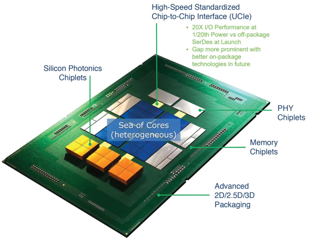
By putting the chiplets inside a multi-die package, it is possible to increase data rates between dies and slash power consumption compared to packages on a board. It becomes possible to assemble multi-die systems whose size far exceeds the largest possible die area of a single die, and whose components can include different kinds of dies—logic chiplets, memory stacks, even analog chiplets—without making huge sacrifices in system speed or power compared to a single-die design. This has become the way forward for CPUs, GPUs, and AI accelerators.
Interconnect is the Root
If a multi-die approach is to succeed, two decisions are crucial. The first is physical materials and structure: how are the dies arranged and mounted, and what material will carry the electrical connections. The second is architectural: how will the chiplets use the connections—masses of independent wires or organized busses—and how will information be transferred—individual bits, parallel words, or serial packet bursts.
Today, the structural question has many possible answers, ranging from simple to remarkably complicated. The simple approach is to mount the bare dies on an organic substrate—the same sort of material used for printed circuit boards, but more specialized. The interconnect wires are printed on the substrate. This organic packaging is mature technology with low costs and resilient global supply chains. Unfortunately, it has also been until recently the most limiting in terms of data rate, energy efficiency, and interconnect density.
The alternative is known as advanced packaging. The most common technique today is to use a silicon substrate or silicon interposers, manufactured using techniques very like those used for the final steps of IC manufacturing. Silicon substrates allow very high densities of wires, high data rates between dies, and low energy per bit transferred. But they can cost over a thousand dollars per unit, with single-source supply chains, and with strict limitations on the size of the substrate. Similarly, TSMC calls their process CoWoS.
Additional advanced techniques include using an organic substrate with bits of silicon embedded in it to bridge between dies (Intel’s Embedded Multi-Die Interconnect Bridge) and 3D, stacking dies on top of each other. The latter technique is used today primarily for tall stacks of high-bandwidth memory (HBM) dies. These techniques also offer high speed and relatively low power.
How to Use the Wires
On a single die, blocks are usually connected by just running a parallel mass of unidirectional wires from one block to the other. And this technique can still work between dies on a silicon substrate, at speeds of a megabit per second or less. To go faster, one has to use a more sophisticated scheme, such as multiple lanes of high-speed serial interfaces. This is the technique used by the PCIe bus at board level.
Some years ago, a working group at Aquantia, later acquired by Marvel Semiconductor, decided to optimize this concept for the shorter, better-controlled interconnect lines between dies on organic substrates. They found that the more controlled environment would allow a considerable simplification and shrinking of the interface circuitry. For instance, the interface could use a single wire for each data lane instead of two-wire differential signaling. Sophisticated modulation schemes such as PAM4 and complex forward error correction were not necessary.
The result was a specification called, rather whimsically, Bunch of Wires (BoW). It includes a PHY spec, but is agnostic about what protocols are used over the interconnect. BoW became an Open Compute Foundation specification for inter-die connections, advancing the use of multi-die packaging in computing.
More recently, a multi-company working group took the concepts of the streamlined BoW PHY and developed it into another proposal: the Universal Chiplet Interconnect Express Bus. UCIe uses a PHY similar to early versions of BoW, but like PCIe adds a protocol layer: this one based on Intel’s Computer Express Link for communications between processors and between processors and memory. It does not, critically, currently support the protocol used by HBM memory. The working group currently includes AMD, ARM, Intel, Nvidia, Qualcomm, and foundries Samsung and TSMC.
UCIe seems to have been initially aimed at advanced packaging, taking advantage of the high-quality interconnect, very short distances, and large numbers of wires available with silicon substrates. It has been adapted to work over organic substrates, but at lower bandwidths per millimeter of die-edge [RF1] and with higher power consumption.
A Significant Alternative
In the meantime, the core of the engineering group from Marvel spun off to found start-up Eliyan Corporation. Primarily, with the goal to focus on a high-performance, bi-directional extension of BoW. The result, now proven in TSMC 5nm silicon, is Nulink. Nulink is also protocol-agnostic, and can use a patented gearbox IP block, available as a chiplet, to connect to existing chiplets without redesign. This allows, for instance, HBM memory stacks to function over organic substrates leveraging Nulink.
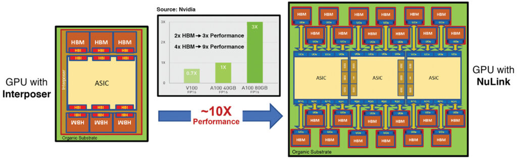
Eliyan has achieved further reductions in size and improvements in performance and efficiency, at twice the bandwidth density of UCIe and half the energy consumption per bit transferred. The speed is similar to UCIe across silicon substrates.
Nonetheless, the real difference between the two technologies emerges on organic substrates, where Nulink achieves twice the data rate of UCIe at less than half the energy per bit. This has profound implications at the system level.
Not only are organic substrates less expensive, with a more resilient supply chain, but their manufacturing process allows them to be much larger than silicon substrates. That larger size means that more devices can be put on one substrate, enjoying the high speed and low power of inter-die connections.
For instance, an AI accelerator package might have two or three massive compute ASICs instead of one. Also, that would still leave room for 24 towers of HBM memory instead of just six, effectively eliminating the memory bottleneck that today restrains the performance of the compute chips.
Moreover, the larger substrate allows for more spacing between dies without loss of performance. This is absolutely critical because HBM dies have a narrow operating temperature range, while GPU and compute ASIC dies are huge heat sources. Added spacing can be the difference between passive conduction cooling and liquid cooling in the package, with major cost, complexity, and reliability benefits at the datacenter level.
It is clear that multi-die packaging is the way forward for the hardware underlying generative AI, and for other massive computing workloads as well. However, silicon substrates remain constrained by high costs, proprietary technologies, and limited substrate area. Achieving silicon-substrate data rates, but with a bidirectional link, at lower energy per bit, with greater bandwidth per millimeter of die-edge width, and over organic substrates removes a major impediment to rapid progress.
Eliyan’s Nulink can increase the performance and reduce the energy consumption of generative AI, giving datacenters a chance to keep up with the accelerating compute loads these applications create.
- Share:


About This Article:
Eliyan Corporation provided the contents of this article.