ASIA ELECTRONICS INDUSTRYYOUR WINDOW TO SMART MANUFACTURING
imec Highlights Potential of Backside Power Delivery
Backside power delivery breaks with the long-standing tradition of processing the signal and power delivery network on the front side of the Si wafer. With backside power delivery, the entire power distribution network is moved to the wafer’s backside. Through-silicon vias (TSVs) bring the power directly from the backside to the front side without the electrons needing to travel through the increasingly complex back-end-of-line (BEOL) stack in the chip’s front side.

Game Changer for Next-Generation Logic
The objective of a backside power delivery network (BSPDN) is decongesting the back-end-of-line (BEOL) in the front side of the logic chip. Also, at the level of the standard cells, it promises a more effective arrangement of the interconnects through design-technology co-optimization (DTCO). This will help to further shrink the size of the logic standard cells. Benefits are also expected at the system level, which increasingly suffers from a rise in power density and an aggressive supply-voltage (or IR) drop. Because backside power-delivering interconnects can be made larger and less resistant, BSPDN is believed to reduce on-chip IR drop significantly. This will facilitate designers to maintain the 10 percent margin allowed for the power loss between the voltage regulator and the transistors. In addition, it holds promises for 3D system-on-chip implementations such as memory on logic, obtained by wafer-on-wafer bonding.
In 2019, imec was the first to propose the concept of backside power delivery and to quantify the advantages at the system level in collaboration with Arm. Meanwhile, BSPDN has entered imec’s roadmap as a context-aware interconnect solution for 2nm and beyond technology nodes. Recently, some major chip manufacturers have announced the introduction of backside power distribution in commercial manufacturing processes of their next-generation logic technologies.
Specific BSPDN Case: nTSVs Landing on Buried Power Rails
BSPDNs bring new process steps and integration challenges to chip processing, including, for example, extreme substrate thinning, micro- or nano-TSV processing, backside to frontside alignment, and backside processing impact on the active front-end-of-line devices. These integration flows, and their challenges are reviewed in a 2023 VLSI invited paper by E. Beyne et al. [1].
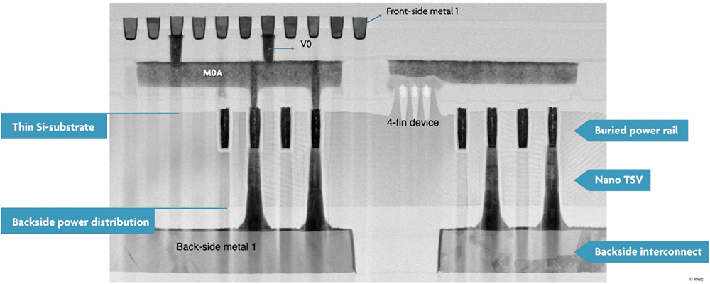
By implementing these process steps, imec experimentally demonstrated one specific implementation of a BSPDN: backside power delivery in combination with buried power rails (BPRs), as shown at VLSI 2022. A BPR is a vertical metallization embedded deep in the chip’s front-end-of-line, running parallel with the standard cells. imec used these BPRs to connect scaled FinFET devices to both backside and front side. Power was delivered from the backside through 320nm deep nTSVs landing on the BPRs at a tight pitch of 200nm without consuming any area of the standard cell. Backside processing did not negatively impact the FinFET devices’ performance in the front end [2].
Block-Level Evaluation: A High-Density vs. High-Performance Case
While the above work looks at the BSPDN and the connectivity of the transistors at the standard cell level, imec and Arm have taken the next step: a zoom out to block level – a representation of a larger part of the integrated circuit – where the benefits of BSPDN can be fully harvested. They investigated whether a BSPDN + BPR implementation brings improved power integrity at the block level compared to frontside PDN implementations.

A block-level evaluation through design-technology co-optimization (DTCO) allows to evaluate the on-chip IR drop, the primary metric for quantifying the power delivery performance. It also gives information on how invasive the PDN is for the integrated circuit by quantifying the PDN’s impact on power, performance, and area (PPA). The study additionally reveals how certain knobs can be tuned to optimize the PDN for a specific operating condition.
BSPDN-based designs were already shown to outperform frontside PDN designs for high-density logic operation conditions. In high-density logic, designs are optimized for maximum power savings and reduced area. For a nanosheet-based device architecture, this can be obtained by keeping the width of the nanosheets as small as possible. But the gains were so far never quantified for high-performance logic. High-performance logic targets fast switching and high drive currents, implementing nanosheet devices with typically larger sheet widths and threshold voltages. Power density requirements are even more stringent than for high-density logic, and, therefore, the benefits of a BSPDN are expected to be even more impactful.
BSPDN + BPR: A block-level PPA Booster
In a paper presented at VLSI 2023, imec and Arm evaluated the impact of a (BS)PDN on a commercial high-performance 64-bit processor block from Arm [3]. Three different PDN implementations were assessed: a traditional frontside implementation, buried power rails with frontside connectivity, and a backside power delivery network with nTSVs landing on buried power rails. A high-performance flavor of the imec A14 nanosheet process design kit (PDK) was developed to guarantee a realistic implementation of the high-performance computing block. An in-house developed analytical model was used in combination with a physical design framework to enable the block-level PPA evaluation and IR drop validation.
The BSPDN simultaneously achieves 6 percent frequency and 16 percent area improvement with no drawback on energy consumption compared to a frontside PDN. Compared to implementing a BPR with frontside connectivity, the BSPDN yields a 2 percent higher frequency on an 8 percent smaller area and a 2 percent energy reduction.

Researchers established a maximum allowable power loss of 35mV for the IR drop evaluation, corresponding to 10% of the nominal voltage supply (VDD + VSS). For the BSPDN implementation, this target was achieved with a relaxed nTSV pitch (4-6µm), representing the pitch at which the power is ‘tapped.’ For both frontside options, however, this target could only be achieved with very tight PDN pitches (or small CPP), negatively impacting the processor’s performance.
The imec team also investigated how the power integrity of the BSPDN case could be further improved, for example, by changing the material used for the nTSVs. The IR drop could be further reduced by 23 percent when using Ru instead of W due to improved nTSV resistance.
In short, the potential of a BSPDN as a block-level PPA booster and IR drop reducer can be fully harvested in a high-performance compute context.
Options for Backside Connectivity at Standard Cell Level
So far, researchers have discussed only one implementation of a BSPDN, where power is brought from the backside to the front side through nTSVs that land on a BPR. From the BPR, a small via connects to the bottom of a middle-of-line (M0A) metallization to access the transistors at the standard cell level.
In addition to this ‘BPR’ approach, researchers are exploring other options for realizing backside power connections at the level of the standard cells. At VLSI 2023, imec discusses two other connectivity schemes for accessing nanosheet transistors [4]. In the TSV-middle approach (TSVM), a tall via in the middle-of-line connects the backside metal-1 to the side of the M0A metal without a buried power rail. In a third and more advanced option, a via directly connects the bottom of the nanosheet’s source-drain epi to the backside metal-1. Of this direct backside connectivity option (BSC), three flavors exist, mainly differing in the size of the contact area. While in BSC-E (epi BSC), the via only connects to the bottom of the source-drain epi, in BSC-M, the via also connects to the metal contact. A third flavor, BSC-M*, extends BSC-M by reducing the gate cut and further increasing the ‘active’ width of the nanosheet (WNS).
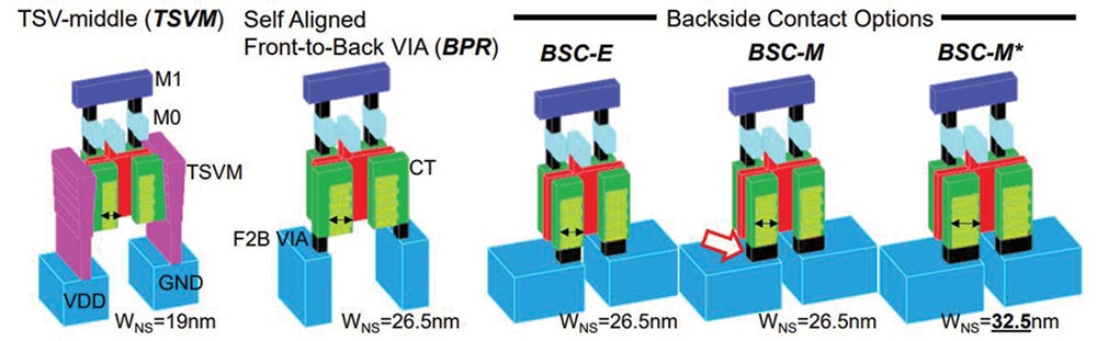
The various connectivity schemes have different properties (such as WNS), with varying impacts on the electrical performance and scaling potential of the standard cells. Generally, when going from TSVM to BPR and BSC, the schemes become increasingly more compact and more challenging to integrate. However, researchers can expect that with further scaling the logic roadmap, the greater integration complexity will be offset by larger gains in terms of PPA.
Toward Direct Backside Connectivity
At VLSI 2023, imec has quantified the PPA and scaling potential of the different backside power options in 2nm and A14 nanosheet technologies for both high-density (2nm, 6T; A14, 5T) and high-performance (2nm 7T; A14 6T) logic conditions [4]. The primary metric for performance evaluation was the simulated frequency of a ring oscillator, expressed as the ratio of the effective drive current and the effective capacitance (Ieff/Ceff).
For high-performance logic at the 2nm node, for the largest, 7T standard cells, there is hardly any difference in frequency between the different connectivity options. When scaling to A14, however, the TSVM approach still survives 6T designs but runs 8.5 percent slower than, e.g., BPR. Overall, BSC-M* clearly outperforms the other options (e.g., 5 percent faster than BPR).
For high-density logic at the 2nm node, which involves even smaller track heights (6T) than high-performance logic, the difference between the frequencies of the different options becomes more pronounced. When scaling to A14 and 5T, TSVM is no longer a viable option, and only BPR and BSC are considered. The relative difference in sheet width between BPR and BSC-M* now weighs more heavily than in 2nm, making BSC-M* the clear winner (8.9 percent faster than BPR).
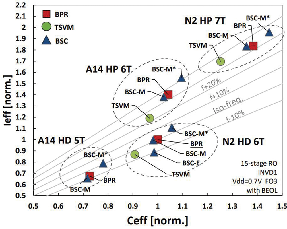
In summary, although TSVM takes more space, it is still a good choice for larger cells, such as in 2nm 7T logic. However, BPR and BSC have a better scaling potential, dimensionally and electrically. The direct backside contact BSC-M* flavor is the clear winner for small track heights due to a larger nanosheet width and contact area than the other options. For BSC-M*, however, the performance gains should be weighed against the larger integration challenge.
The imec team is currently working on a technology demonstration of the different backside connectivity options and, in collaboration with Arm, on a block-level PPA evaluation.
Beyond Backside Power Delivery
While the backside of the Si wafer remained unused for a long time, the first instantiation of utilizing the backside will be for power delivery. In parallel, imec and its partners from industry explore which other functionalities can be migrated to the backside as well. Think, for example, of global interconnects and clock signal distribution. While power delivery is a very specific type of interconnect optimized for minimal resistance, distributing clock or other types of signals may have different properties, changing the way the backside will be addressed. Imec is currently investigating what challenges and opportunities this functional backside – or backside 2.0 – may bring along.
The VLSI 2023 papers are available upon request through imec. Interested parties may contact imec at https://www.imec-int.com/en/connect-with-us.
About this Article
The author is Julien Ryckaert, Vice President of Logic and in charge of Compute Scaling at imec. Ryckaert received an M.Sc. degree in electrical engineering from the University of Brussels (ULB), Belgium, in 2000 and a Ph.D. degree from the Vrije Universiteit Brussel (VUB) in 2007.
Notes:
[1] ‘Nano-through silicon vias (nTSV) for backside power delivery networks (BSPDN)’, E. Beyne et al., VLSI 2023, invited paper;
[2] ‘Imec demonstrates backside power delivery with buried power rails for back- and frontside routing’, Press release, VLSI 2022;
[3] ‘Block-level evaluation and optimization of backside PDN for high-performance computing at the A14 node’, G. Sisto et al., VLSI 2023;
[4] ‘PPA and scaling potential of backside power options in N2 and A14 nanosheet technology’, S. Yang et al., VLSI 2023.
- Share: